Light sensing module packaging structure
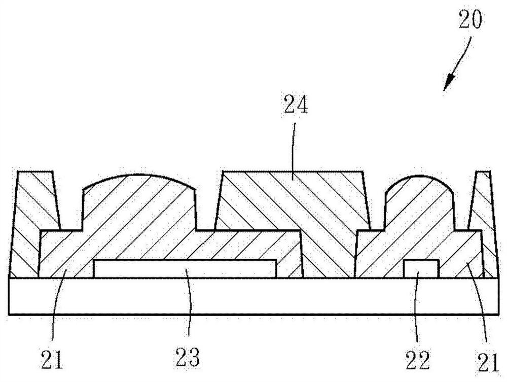
A light-sensing module and packaging structure technology, applied in the direction of electrical components, electric solid-state devices, circuits, etc., can solve the needs of shrinking the size of the packaging structure 20, reducing the stability of the light-sensing chip 23, and failing to meet the needs of thinning products And other issues
- Summary
- Abstract
- Description
- Claims
- Application Information
AI Technical Summary
Problems solved by technology
Method used
Image
Examples
Embodiment Construction
[0030] The applicant hereby explains that throughout the specification, including the following embodiments and the claims of the scope of patent protection, terms related to direction are all based on the directions in the drawings. Secondly, in the embodiments to be described below and in the accompanying drawings, the same component numbers represent the same or similar components or their structural features. Not drawn in actual form.
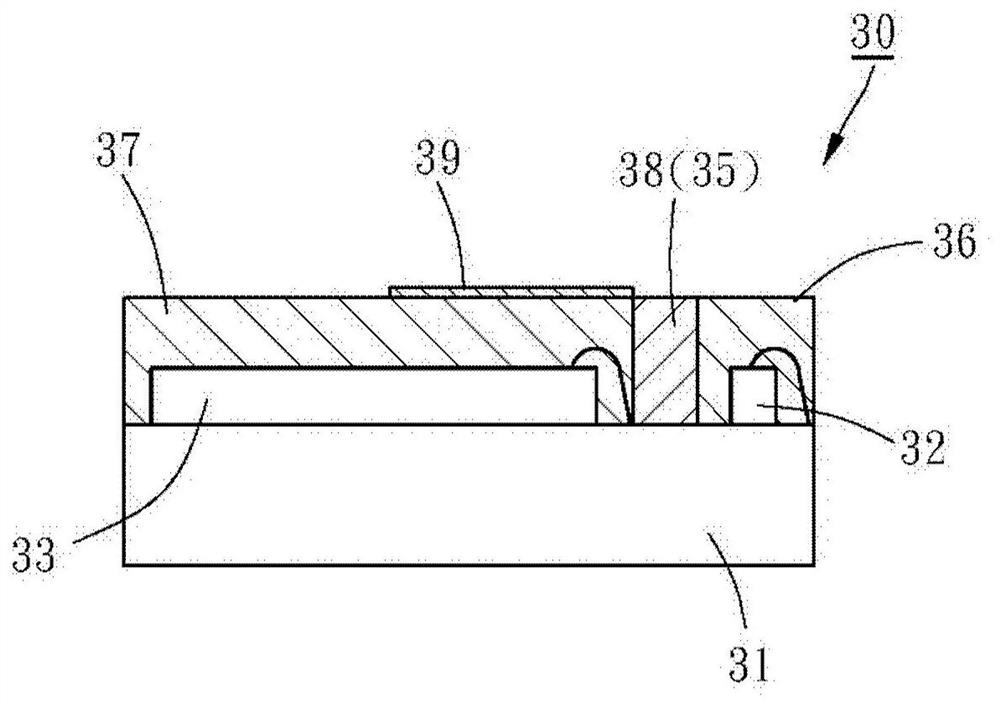
[0031] see image 3 and Figure 4 The package structure 30 of the photo-sensing module of the present invention includes a substrate 31, a light-emitting element 32, a photo-sensing chip 33, an encapsulant 34, a first light-blocking layer 38, and a second light-blocking layer 39 .
[0032] The substrate 31 may be a printed circuit board, a BT substrate, an FR-4 epoxy glass fiber substrate or a direct copper clad substrate, which is not limited here.
[0033] Such as Figure 5 As shown in step S1, the light-emitting element 32 (here, a ...
PUM
 Abstract
Description
Claims
Application Information


