Display panel and spliced screen

A technology of display panel and display area, applied in the direction of instruments, electrical components, electrical solid devices, etc., can solve the problems affecting the display effect of the splicing screen, the width of the frame, etc.

Pending Publication Date: 2020-10-20
TCL CHINA STAR OPTOELECTRONICS TECH CO LTD
View PDF7 Cites 6 Cited by
  • Summary
  • Abstract
  • Description
  • Claims
  • Application Information

AI Technical Summary

Problems solved by technology

[0005] The application provides a display panel and a splicing screen, which can solve the technical problem that the frame of the traditional display panel is wide and affects the display effect of the splicing screen

Method used


Image

  • Display panel and spliced screen
  • Display panel and spliced screen
  • Display panel and spliced screen

Examples


Embodiment 1

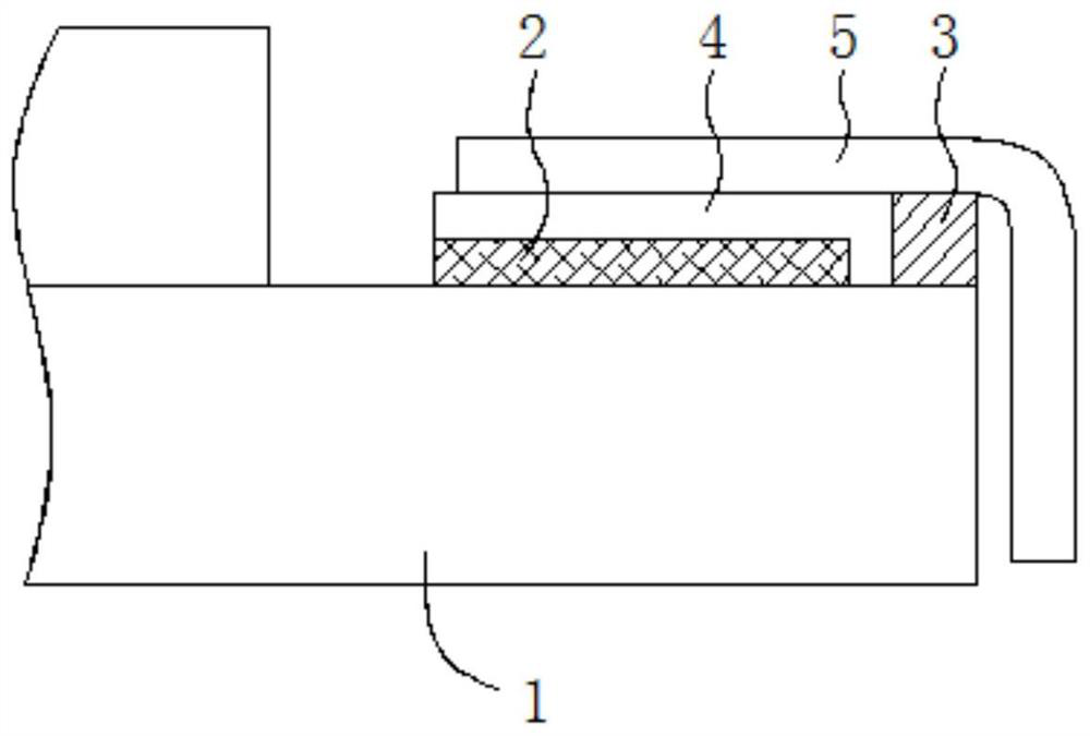
[0033] Please combine figure 1 and figure 2 As shown, in this embodiment, at least two of the binding pads 2 are arranged in a one-dimensional manner along the boundary of the display panel, and the retaining wall 3 is arranged on the binding pads 2 close to the boundary of the display panel side. Wherein, the length of the retaining wall 3 in the direction in which the binding pads 2 are arranged is greater than the length of the arrangement of the binding pads 2 . It can be understood that if there are M binding pads 2, wherein M is a positive integer greater than or equal to 2, the arrangement length of the binding pads 2 is the first binding pad from left to right. The distance between the left end of pad 2 and the right end of the Mth bonding pad 2. Therefore, setting the length of the retaining wall 3 to be greater than the arrangement length of the bonding pads 2 can ensure that the retaining wall 3 can have a good barrier performance.

[0034] In this embodiment, ...

Embodiment 2

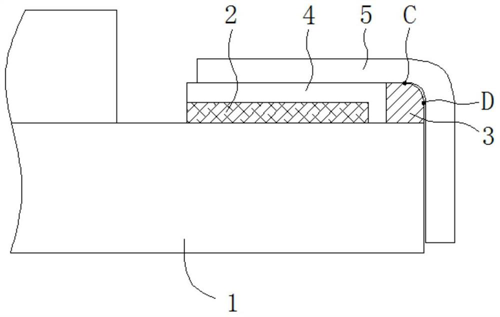
[0046] Please refer to image 3 As shown in , it is a schematic structural diagram of the display panel provided in Embodiment 2 of the present application. The difference between the display panel of this embodiment and the first embodiment above is that: in this embodiment, the barrier wall 3 has a curved surface on the side close to the boundary of the display panel, and the chip-on-chip film 5 corresponds to outside the binding area. A portion is bent along the curved surface of the retaining wall 3 to the side of the display panel.

[0047] like image 3 As shown in , the section of the retaining wall 3 has an arc segment CD, and the surface of the bent portion of the COF 5 is in close contact with the arc segment CD. Due to the design of the arc segment CD, it can be The bending portion of the COF 5 avoids a certain space, which is convenient for the bending of the COF 5, so that the part of the COF 5 bent to the side of the display panel is arranged close to the side ...


PUM


Abstract

The invention provides a display panel and a spliced screen. The display panel comprises a display area and a binding area located on one side of the display area. The display panel also comprises a binding bonding pad which is arranged in the binding area, a retaining wall which is arranged on one side, close to the boundary of the display panel, of the binding bonding pad; and a chip-on-film which is bound on the binding bonding pad through a conductive adhesive; wherein a signal line of the display area is electrically connected with the binding bonding pad; and the boundary of the conductive adhesive is located on the side, close to the display area, of the retaining wall. According to the invention, the retaining wall is arranged on the edge of the display panel, so that the problem of conductive adhesive overflowing caused by the binding of the chip-on-film and the display panel is prevented, the frame width of the display panel is reduced, and the display effect of the spliced screen is improved.

Description

technical field [0001] The present application relates to the field of display technology, in particular to a display panel and a splicing screen. Background technique [0002] With the rapid development of flat panel display technology, its size and application scenarios are constantly expanding, and various manufacturers have launched larger-sized display panels. Due to the limitation of the production process, when the size of the display panel cannot be made larger, a spliced ​​display device emerges as the times require. Because it has a large-scene display effect and can bring users an immersive visual experience, the splicing display device is widely used in various occasions such as advertisements, publicity, and exhibitions. [0003] Although various techniques are used in the prior art to minimize peripheral circuits in order to improve the display quality, there are still some factors that affect the frame width of the display panel. For example, when the chip-o...

Claims


Application Information

Patent Timeline
Patent Type & Authority Applications(China)
IPC IPC(8): G09F9/30G09F9/35G09F9/302H01L27/32
CPCG09F9/30G09F9/35G09F9/3026H10K59/10
Inventor 徐健
Owner TCL CHINA STAR OPTOELECTRONICS TECH CO LTD
Why Eureka
Try Eureka