Method and device for starting process task in semiconductor process equipment

A technology of process equipment and semiconductors, which is applied in semiconductor/solid-state device manufacturing, electrical components, circuits, etc., and can solve problems such as deadlocks

Pending Publication Date: 2020-11-13
BEIJING NAURA MICROELECTRONICS EQUIP CO LTD
View PDF0 Cites 5 Cited by
  • Summary
  • Abstract
  • Description
  • Claims
  • Application Information

AI Technical Summary

Problems solved by technology

lead to a dead

Method used


Image

  • Method and device for starting process task in semiconductor process equipment
  • Method and device for starting process task in semiconductor process equipment
  • Method and device for starting process task in semiconductor process equipment

Examples


Embodiment Construction

[0028] The application will be further described in detail below in conjunction with the accompanying drawings and embodiments. It should be understood that the specific embodiments described here are only used to explain related inventions, rather than to limit the invention. It should also be noted that, for the convenience of description, only the parts related to the related invention are shown in the drawings.

[0029] It should be noted that, in the case of no conflict, the embodiments in the present application and the features in the embodiments can be combined with each other. The present application will be described in detail below with reference to the accompanying drawings and embodiments.

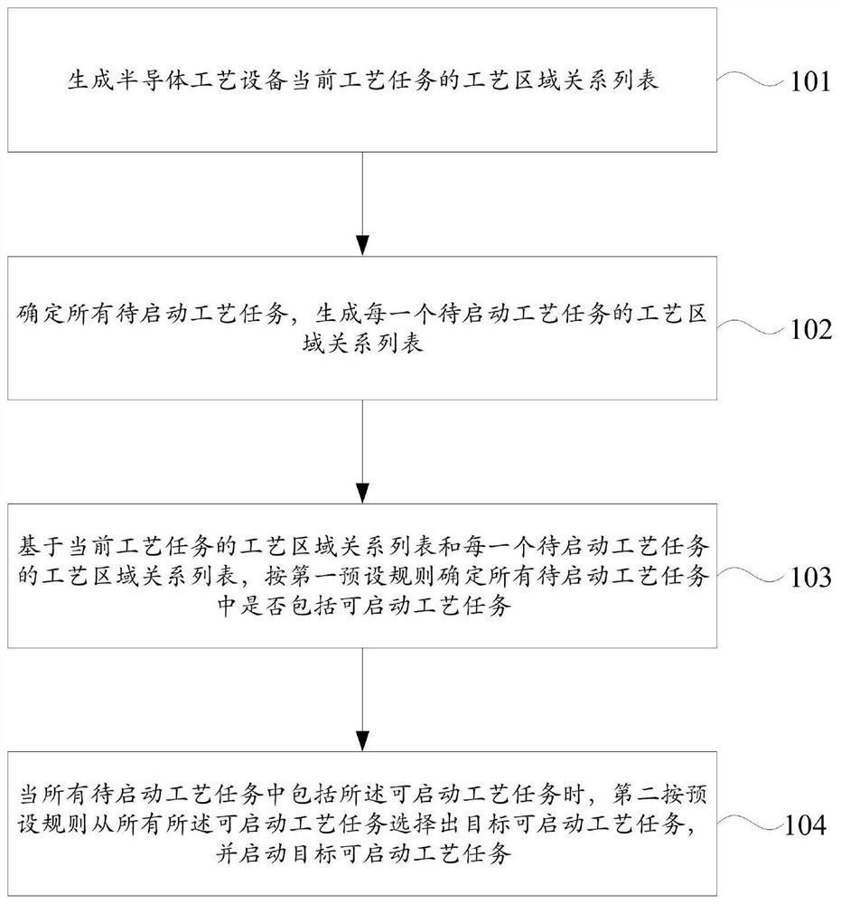
[0030] figure 1 A flowchart of a first embodiment of a method for starting a process task in a semiconductor process equipment provided in an embodiment of the present application is shown, and the method includes:

[0031] Step 101 , generating a process area relationship ...


PUM


Abstract

The invention provides a method and a device for starting a process task in semiconductor process equipment. The method comprises the steps of generating a process region relationship list of a current process task of the semiconductor process equipment; determining all to-be-started process tasks, and generating a process region relationship list of each to-be-started process task; based on the process area relationship list of the current process task and the process area relationship list of each to-be-started process task, determining whether all the to-be-started process tasks include startable process tasks or not according to a first preset rule; and when all the to-be-started process tasks include the startable process tasks, selecting a target startable process task from all the startable process tasks according to a second preset rule, and starting the target startable process task. Therefore, the situation that the target startable process task and the current process task aim at materials in two same process areas but are opposite in sequence does not occur at any moment, deadlock is avoided, and the production efficiency is improved.

Description

technical field [0001] The present application relates to the technical field of semiconductor equipment, in particular to a method and device for starting process tasks in semiconductor process equipment. Background technique [0002] A deadlock situation is an abnormal situation that has the greatest influence on the work efficiency of the semiconductor process equipment in the case of performing multitasking in the semiconductor process equipment such as a wafer cleaning equipment. The occurrence of a deadlock will cause the downtime of the semiconductor process equipment, affect the output of the semiconductor process equipment, and cause the semiconductor process equipment to fail to work normally. [0003] Taking the wafer cleaning equipment as an example, for the first task and the second task whose start time is close, the out-of-order RouteRecipe of the first task is expressed as: Shelf–PDO1 / PDO2–WTC–IOBuffer–Tank1-Tank2–Tank7-Tank8–Dry –WTC–PDO1 / PDO2–Shelf. The s...

Claims


Application Information

Patent Timeline
IPC IPC(8): H01L21/02H01L21/67
CPCH01L21/67253H01L21/67276H01L21/02057H01L21/67207H01L21/67028Y02P90/02G06Q10/06G05B19/41865
Inventor 吴芳娜史思雪
Owner BEIJING NAURA MICROELECTRONICS EQUIP CO LTD
Why Eureka
Try Eureka