Test structure and its test method

A technology for testing structures and testing methods, applied in semiconductor/solid-state device testing/measurement, electronic circuit testing, electrical measurement, etc., can solve the passivation layer crack, evaluate the internal stress of the passivation layer, detect the passivation layer crack, etc. problem, to achieve the effect of sensitive detection

Active Publication Date: 2020-12-25
晶芯成(北京)科技有限公司
View PDF5 Cites 0 Cited by
  • Summary
  • Abstract
  • Description
  • Claims
  • Application Information

AI Technical Summary

Problems solved by technology

However, a large internal stress is often generated in the passivation layer, and it is easy to cause the passivation layer to break under the large internal stress.
[0003] In the current common semiconductor manufacturing process, there is no corresponding test structure to detect whether the passivation layer is cracked, and there is no suitable test structure for evaluating the internal stress of the passivation layer

Method used


Image

  • Test structure and its test method
  • Test structure and its test method
  • Test structure and its test method

Examples


Embodiment Construction

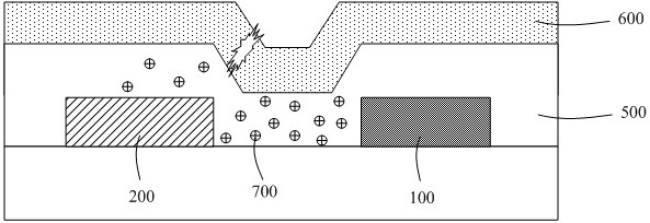
[0050] As mentioned in the background art, the film integrity of the passivation layer plays an extremely important role for the entire chip or device. Therefore, how to judge the integrity of the passivation layer and evaluate the internal stress of the passivation layer is particularly necessary.

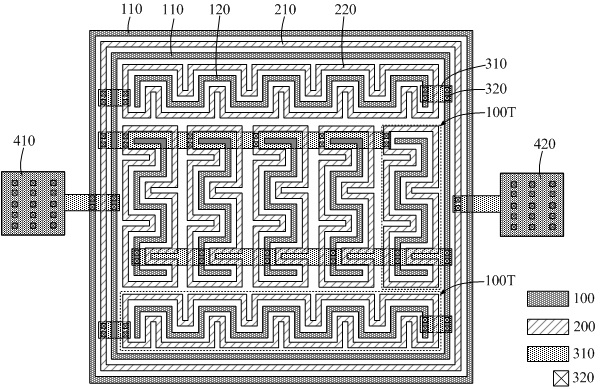
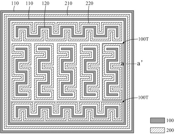
[0051] In view of the above technical problems, the present invention mainly obtains a test structure for detecting the integrity of the passivation layer by performing circuit layout on the metal layer immediately below the passivation layer.

[0052] In addition, the present invention also finds that the circuit layout of the metal layer immediately below the passivation layer will affect the stress distribution of the passivation layer. The circuit layout of the metal layer is improved so that the internal stress of the passivation layer can also be evaluated by using the test structure of the present invention.

[0053] The test structure and test method proposed by the prese...


PUM


Abstract

The invention provides a test structure and a test method thereof. A first metal layer is arranged below a passivation layer; a first conductive path and a second conductive path are formed in the first metal layer; the first metal layer is further filled with a dielectric layer allowing alkali ions to diffuse, so that whether the alkali ions diffuse in the dielectric layer between the first conductive path and the second conductive path or not can be judged through an electrical test, and then whether the passivation layer is broken or not can be deduced. According to the test structure provided by the invention, the integrity of the passivation layer can be sensitively detected, and the stress of the passivation layer can be evaluated by adjusting the circuit layout of the first metal layer.

Description

technical field [0001] The invention relates to the technical field of semiconductors, in particular to a test structure and a test method thereof. Background technique [0002] In semiconductor manufacturing, in order to protect the chip from external environmental moisture, ionic contamination, chemical hazards and mechanical stress, a passivation layer (Passivation) is usually deposited on the surface of the chip to isolate the structure below the passivation layer Protect. However, relatively large internal stress is often generated in the passivation layer, and the passivation layer is easily broken under the relatively large internal stress. [0003] In the current common semiconductor manufacturing process, there is no corresponding test structure to detect whether the passivation layer is cracked, and there is no suitable test structure for evaluating the internal stress of the passivation layer. Contents of the invention [0004] The purpose of the present inven...

Claims


Application Information

Patent Timeline
Patent Type & Authority Patents(China)
IPC IPC(8): H01L23/544H01L21/66G01R31/28
CPCG01R31/2872G01R31/2874G01R31/2879H01L22/12H01L22/30H01L22/32
Inventor 周山王丽雅俞佩佩
Owner 晶芯成(北京)科技有限公司
Why Eureka
Try Eureka