OLED display panel and display device
A display panel and display area technology, which is applied to semiconductor devices, electrical components, circuits, etc., can solve the problems affecting the display effect of OLED display panels, and achieve the effect of improving the display effect.
- Summary
- Abstract
- Description
- Claims
- Application Information
AI Technical Summary
Problems solved by technology
Method used
Image
Examples
Embodiment 1
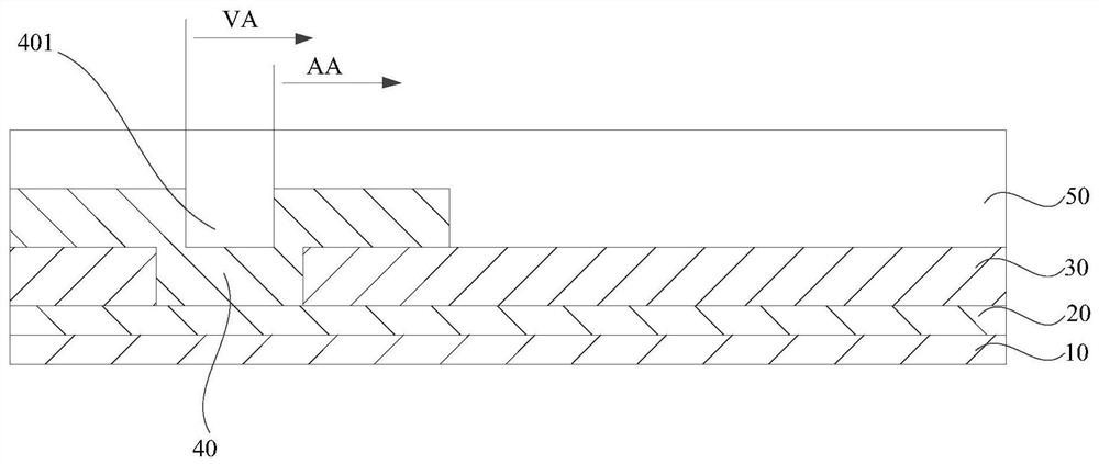
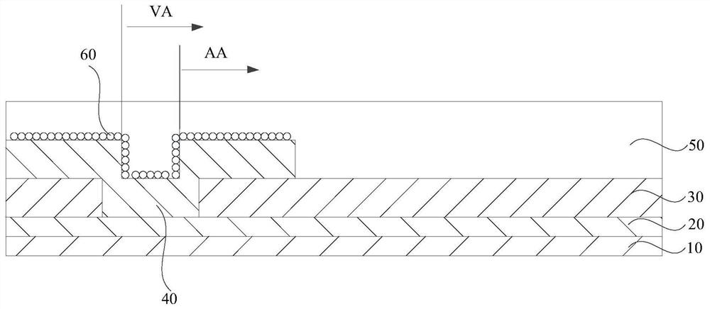
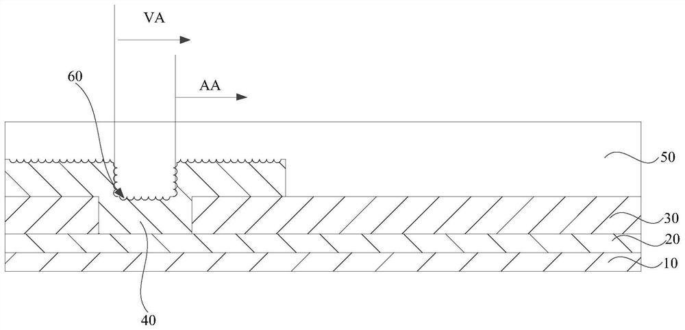
[0045] In this embodiment, the visible area is represented by VA, and the display area is represented by AA. like figure 2 As shown, the OLED display panel provided by the embodiment of the present invention includes: a visible area VA and a display area AA located in the visible area VA. The viewing area VA is an area that can be seen by the human eye after the device is installed, and the display area AA is an area where a touch operation can be performed in the visual area VA to perform a corresponding function.
[0046] The OLED display panel includes a substrate 10 , a conductive layer 20 disposed on one side of the substrate 10 , an insulating layer 30 disposed on the side of the conductive layer 20 away from the substrate 10 , and an insulating layer 30 disposed on the side of the insulating layer 30 away from the conductive layer 20 . The electrode layer 40, and the cover plate 50 disposed on the electrode layer 40 and away from the substrate 10, wherein the insulati...
Embodiment 2
[0062]This embodiment only describes the parts that are different from the first embodiment, and the structural parts that are the same as those of the first embodiment will not be repeated in this embodiment.
[0063] like Figure 4 As shown, in the OLED display panel provided by the embodiment of the present invention, the microstructure film layer is a semi-transparent and semi-reflective film layer 70, along the first direction parallel to the touch surface of the display area AA (in this embodiment, the first direction Denoted by B, that is, the first direction B), and on the same side of the visible area VA and the display area AA, the semi-transparent and semi-reflective film layer 70 is disposed between the edge of the visible area VA and the edge of the display area AA.
[0064] It should be noted that the edges of the visible area VA and the display area AA on the same side refer to the fact that both edges are located on the same side of the display panel.
[0065]...
Embodiment 3
[0077] An embodiment of the present invention further provides a display device, including the OLED display panel provided in the first embodiment and the second embodiment.
[0078] The working principle and structure of the OLED display panel have been described in detail in the above embodiments, and are not repeated in this embodiment.
[0079] The display device provided by the embodiment of the present invention includes an OLED display panel, wherein the OLED display panel is provided with a microstructure film layer between the electrode layer and the cover plate, wherein at least part of the microstructure film layer is projected on the substrate Coinciding with the projection of the groove on the substrate, when light from the top of the OLED display panel strikes the groove, the microstructure film layer can reduce the reflection intensity of the light in the groove, so that the light enters the groove. When the light of the OLED is reflected from the groove, the pu...
PUM
 Abstract
Description
Claims
Application Information


