Optical structure film for carrying out electrode patterning on silver nanowire transparent conductive film and patterning method of optical structure film

A technology of transparent conductive film and optical structure, applied in electrical digital data processing, data processing input/output process, coating and other directions, can solve the problems of serious etching marks and silver migration of nano silver wire transparent conductive film, and achieve good Optical performance and stability, enhanced fluidity, and the effect of eliminating silver migration problems

Active Publication Date: 2020-11-17
合肥微晶材料科技有限公司
View PDF6 Cites 0 Cited by
  • Summary
  • Abstract
  • Description
  • Claims
  • Application Information

AI Technical Summary

Problems solved by technology

[0006] Aiming at the problems existing in the above-mentioned prior art, the present invention provides an optical structure film and a patterning method for electrode patterning of silver nanowire transparent conductive film, in order to effectively solve the problem of etching of transparent conductive film of silver nanowire. Severe marks and problems of silver migration

Method used


Image

  • Optical structure film for carrying out electrode patterning on silver nanowire transparent conductive film and patterning method of optical structure film
  • Optical structure film for carrying out electrode patterning on silver nanowire transparent conductive film and patterning method of optical structure film
  • Optical structure film for carrying out electrode patterning on silver nanowire transparent conductive film and patterning method of optical structure film

Examples


Embodiment 1

[0076] The UV hardening solution formula used in this embodiment is as follows:

[0077]

[0078] The specific preparation method is: weigh each raw material according to the proportion, first add pentaerythritol tetraacrylate to CN8885NS resin, stir at 500r / min for 25min, then add dodecyl mercaptan, light stabilizer 292, BYK- 333 and photoinitiator 754, continue to stir for 20 minutes to obtain UV hardening solution.

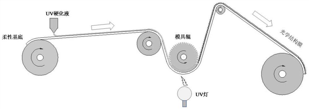
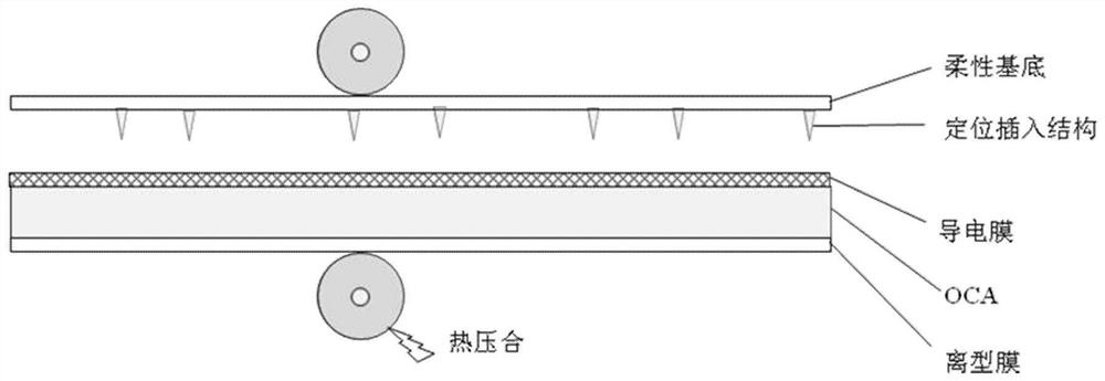
[0079] Such as figure 1 As shown, based on the above-mentioned UV hardening solution, an optical structure film is produced in this embodiment:

[0080] Firstly, the UV hardening solution is coated on the surface of the flexible substrate PET through the dimple coating process;

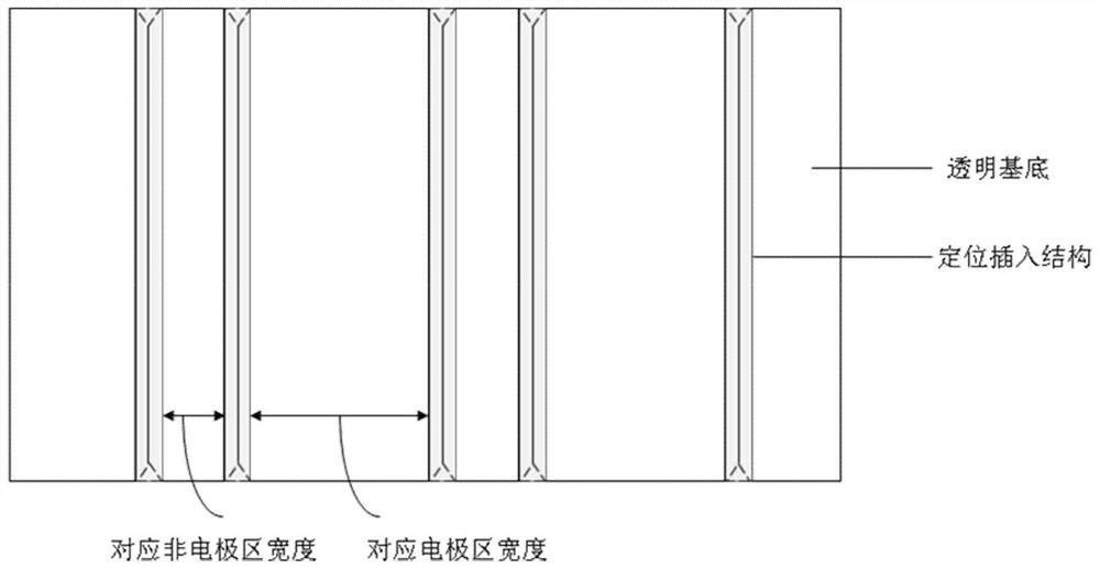
[0081] The UV hardening solution on the surface of the flexible substrate is then embossed using a mold roll with the desired pattern (made in advance by an electron beam etching process) to form a positioning insertion structure of the desired pattern;

[0082] Finally, UV curin...

Embodiment 2

[0088] This embodiment is the same as Embodiment 1, the only difference is that the UV hardening liquid formula used is as follows:

[0089]

Embodiment 3

[0091] This embodiment is the same as Embodiment 2, the only difference is that the UV hardening liquid formula used is as follows:

[0092]

[0093] Table 1 shows the performance comparison results of the silver nanowire transparent conductive film obtained in the above examples and comparative examples after electrode patterning.

[0094] Table 1: Comparison of the performance of the patterned conductive film obtained in the comparative example and each embodiment

[0095]

[0096]

[0097] It can be seen from Table 1 that the optical structure layer in the silver nano wire flexible transparent conductive film of the present invention does not affect the performance of the conductive film, and the etching marks of the silver nano wire conductive film of the embodiment are obviously improved.


PUM


Abstract

The invention discloses an optical structure film for performing electrode patterning on a silver nanowire transparent conductive film and a patterning method of the optical structure film. An opticalstructure film with a positioning insertion structure and a silver nanowire transparent conductive film which is transferred to OCA optical cement in advance are subjected to thermocompression bonding, so that the high-hardness positioning insertion structure is embedded into the silver nanowire conductive film to realize electrode patterning of the conductive film so as to prepare a required conductive electrode pattern. According to the method, the problems of silver migration and etching marks of the silver nanowire transparent conductive film can be effectively solved, and the method is simple and high in reliability.

Description

technical field [0001] The invention belongs to the field of nano-silver wire transparent conductive films, in particular to an optical structure film and a patterning method for electrode patterning of nano-silver wire transparent conductive films. Background technique [0002] The application of nano-silver wire transparent conductive film in the field of touch control is becoming more and more mature. It needs to be processed by electrode patterning, and then laminated with optical transparent adhesive to form a composite film, and then laminated with liquid crystal display module or OLED display module. Made into a touch screen. The electrode patterning method is mainly laser etching, that is, using laser to remove part of the conductive film between the electrode area and the non-electrode area, so as to separate the electrode area from the non-electrode area. The diameter of the laser beam is 25-35 μm. Therefore, the distance between the electrode patterns made by las...

Claims


Application Information

Patent Timeline
IPC IPC(8): C09D175/14G06F3/041
CPCC09D175/14G06F3/041G06F2203/04103
Inventor 张梓晗吕鹏姚成鹏张运奇聂彪
Owner 合肥微晶材料科技有限公司
Why Eureka
Try Eureka