Semiconductor memory device and method of forming the same
A storage device, semiconductor technology, applied in the direction of semiconductor devices, semiconductor/solid-state device manufacturing, transistors, etc.
- Summary
- Abstract
- Description
- Claims
- Application Information
AI Technical Summary
Problems solved by technology
Method used
Image

Examples
Embodiment Construction
[0023] In order to enable those who are familiar with the technical field of the present invention to further understand the present invention, several preferred embodiments of the present invention are enumerated below, and in conjunction with the accompanying drawings, the constitutional content and intended achievement of the present invention are explained in detail. effect.
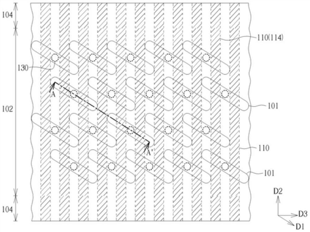
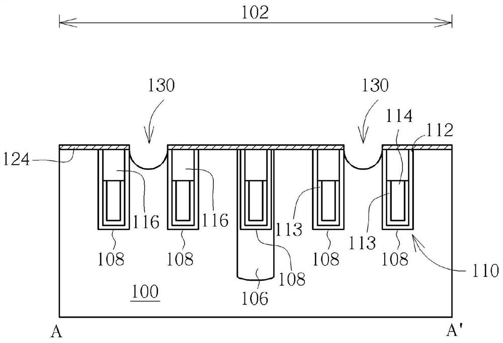
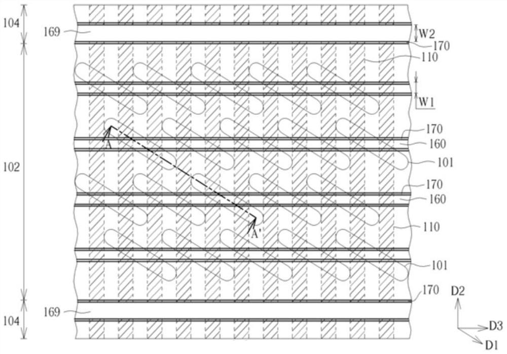
[0024] Please refer to Figure 1 to Figure 7 , which is a schematic diagram of a method for forming a semiconductor storage device in the first preferred embodiment of the present invention, wherein, figure 1 , image 3 and Figure 5 It is a schematic top view of a semiconductor storage device in a manufacturing process, figure 2 , Figure 4 and Figure 6 respectively figure 1 , image 3 and Figure 5 A schematic cross-section along the tangent line A-A' in .
[0025] In this embodiment, the semiconductor storage device is, for example, a recessed gate random dynamic processing memory (dyn...
PUM
 Abstract
Description
Claims
Application Information
 - R&D Engineer
- R&D Manager
- IP Professional
- Industry Leading Data Capabilities
- Powerful AI technology
- Patent DNA Extraction
Browse by: Latest US Patents, China's latest patents, Technical Efficacy Thesaurus, Application Domain, Technology Topic.
© 2024 PatSnap. All rights reserved.Legal|Privacy policy|Modern Slavery Act Transparency Statement|Sitemap