Light emitting diode and manufacturing method thereof

A technology of light-emitting diodes and light-emitting layers, applied in electrical components, circuits, semiconductor devices, etc., can solve problems such as infiltration into light-emitting diodes, short circuits, etc.

Pending Publication Date: 2020-08-25
GENESIS PHOTONICS
View PDF0 Cites 0 Cited by
  • Summary
  • Abstract
  • Description
  • Claims
  • Application Information

AI Technical Summary

Problems solved by technology

However, during the process of eutectic bonding, the bonding material (for example: solder paste) easily penetrates into the light emitting diode from the interface between the second insulating layer and the first bonding layer and / or the interface between the second insulating layer and the second bonding layer, causing a short circuit

Method used


Image

  • Light emitting diode and manufacturing method thereof
  • Light emitting diode and manufacturing method thereof
  • Light emitting diode and manufacturing method thereof

Examples


Embodiment Construction

[0295] Reference will now be made in detail to the exemplary embodiments of the present invention, examples of which are illustrated in the accompanying drawings. Wherever possible, the same reference numbers will be used in the drawings and description to refer to the same or like parts.

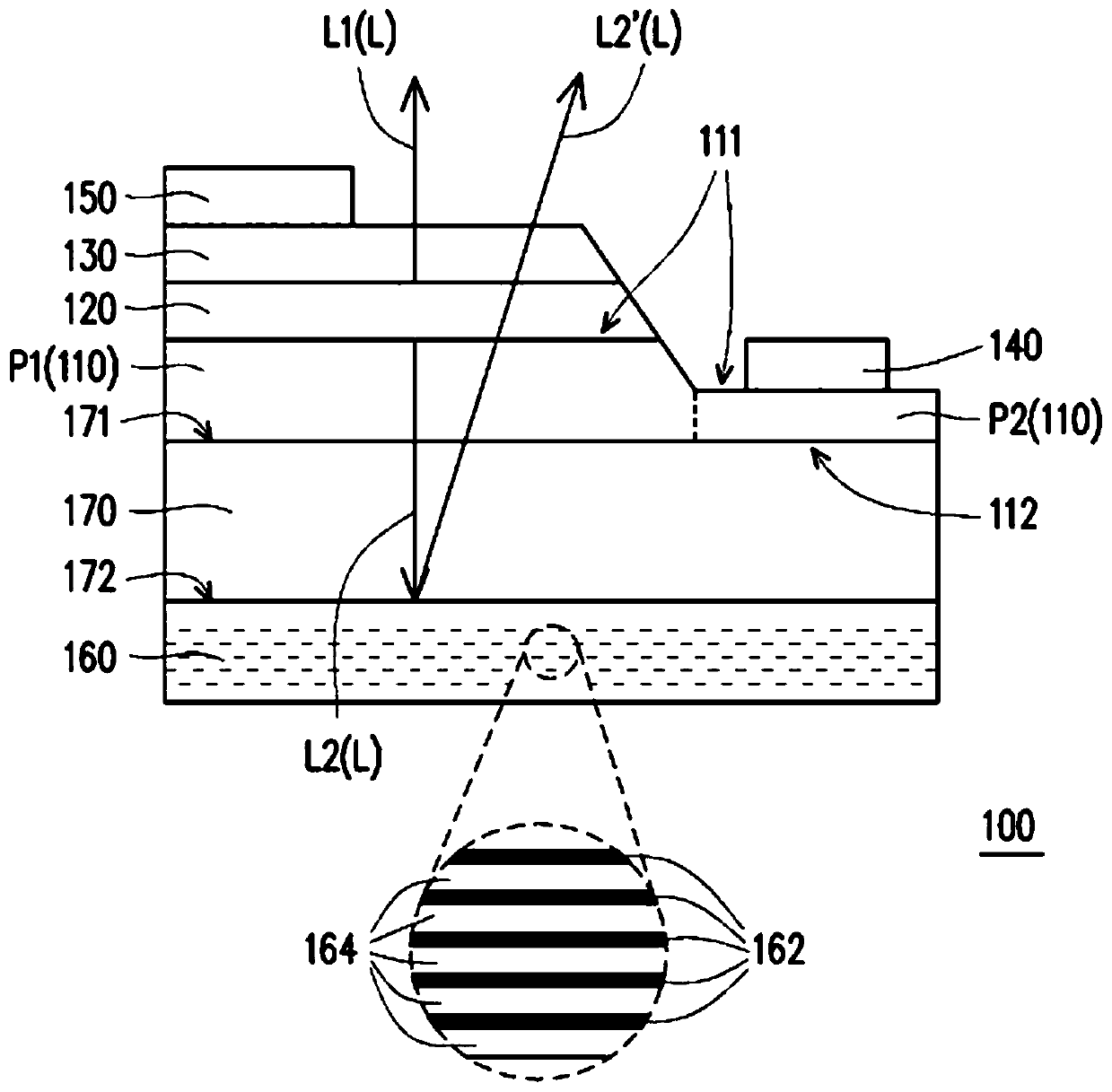
[0296] Figure 1A A cross-sectional view of a light emitting diode according to an embodiment of the present invention is shown. Please refer to Figure 1A ,in particular, Figure 1A Shown is a horizontal LED, and is one type of LED that can be applied to wire bonded packages. The light emitting diode 100 includes a first type semiconductor layer 110 , a light emitting layer 120 , a second type semiconductor layer 130 , a first current conducting layer 140 , a second current conducting layer 150 and a Bragg reflection structure 160 . In this embodiment, one of the first-type semiconductor layer 110 and the second-type semiconductor layer 130 is an N-type semiconductor layer (for example, ...


PUM

PropertyMeasurementUnit
thicknessaaaaaaaaaa
reflectanceaaaaaaaaaa

Abstract

The invention provides a light emitting diode and a manufacturing method thereof. The light emitting diode comprises a first type semiconductor layer, a light emitting layer, a second type semiconductor layer, a first metal layer, a first current conduction layer, a first bonding layer and a second current conduction layer. The light emitting layer is located between the first type semiconductor layer and the second type semiconductor layer. The first metal layer is located on the first type semiconductor layer and is electrically connected with the first type semiconductor layer. The first metal layer is located between the first current conduction layer and the first type semiconductor layer. The first current conducting layer is located between the first bonding layer and the first metal layer. The first bonding layer is electrically connected with the first type semiconductor layer through the first current conduction layer and the first metal layer. The first bonding layer has a through opening overlapping the first metal layer. The second current conduction layer is electrically connected with the second type semiconductor layer.

Description

technical field [0001] The invention relates to a semiconductor element and a manufacturing method thereof, in particular to a light emitting diode and a manufacturing method thereof. Background technique [0002] In general, light emitting diodes include light emitting diodes applied in vertical packaging and flip chip packaging. A light-emitting diode applied to a flip-chip package includes a first-type semiconductor layer, a light-emitting layer, a second-type semiconductor layer, a first metal layer, a second metal layer, a first insulating layer, a first current conducting layer, and a second current conducting layer. layer, a second insulating layer, a first bonding layer, and a second bonding layer. The first type semiconductor layer has a first part and a second part. The light emitting layer is configured on the first part of the first type semiconductor layer. The second part of the first type semiconductor layer extends outward from the first part and protrudes...

Claims


Application Information

Patent Timeline
Patent Type & Authority Applications(China)
IPC IPC(8): H01L33/10H01L33/12H01L33/00
CPCH01L33/12H01L33/10H01L33/005
Inventor 黄逸儒郭佑祯许圣宗沈志铭李耀唐庄东霖黄琮训黄靖恩
Owner GENESIS PHOTONICS
Why Eureka
Try Eureka