

Red light quasi-two-dimensional perovskite light-emitting diode with dication structure
A light-emitting diode, perovskite technology, applied in semiconductor devices, electrical components, circuits, etc., can solve the problems of quasi-two-dimensional thin film brightness and external quantum efficiency decline, poor PLQY, limiting device performance, etc., to reduce exciton quenching. Recombination problem of extinction and non-radiation, high PLQY, the effect of reducing leakage current loss
Active Publication Date: 2020-12-04
JILIN UNIV
View PDF7 Cites 2 Cited by
- Summary
- Abstract
- Description
- Claims
- Application Information
AI Technical Summary
Problems solved by technology
Three-dimensional perovskites (such as MAPbI 3 ) films usually have various non-radiative recombination channels caused by defects or pinholes, which severely limit the device performance
H
Method used
View moreImage
Smart ImageViewing Examples

Examples
 PUM
| Property | Measurement | Unit |
|---|---|---|
| Thickness | aaaaa | aaaaa |
| Thickness | aaaaa | aaaaa |
| Thickness | aaaaa | aaaaa |
Abstract
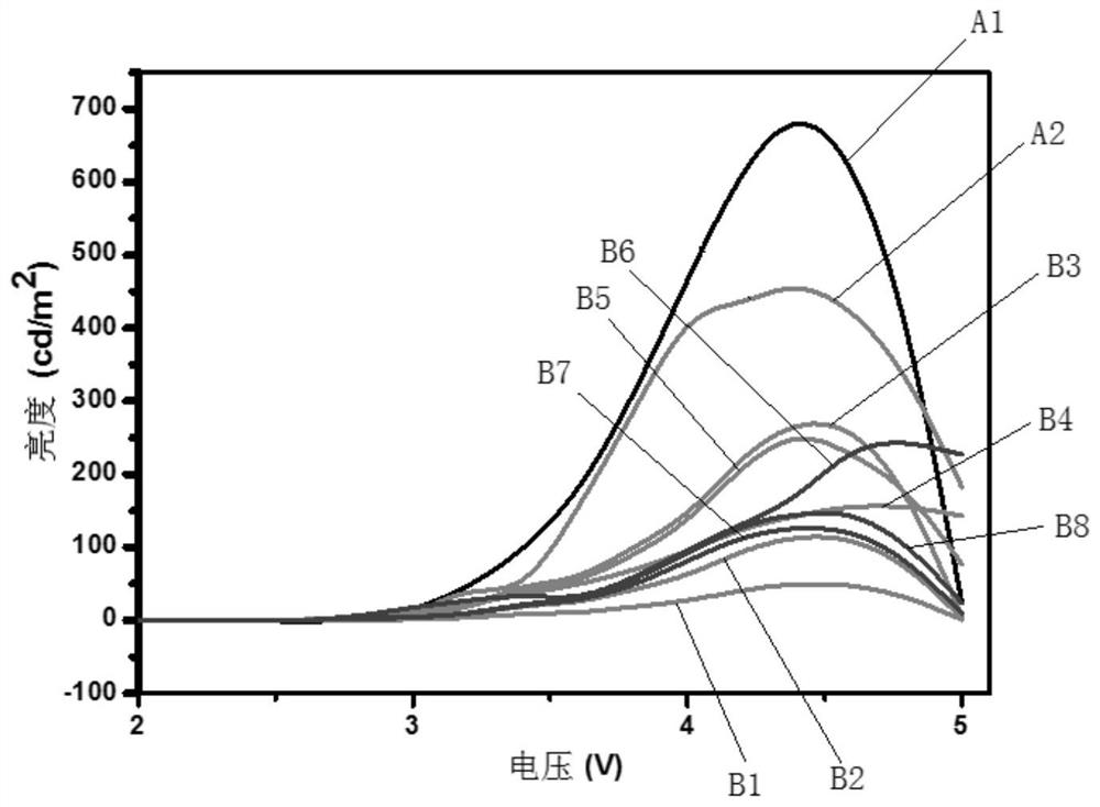
The invention relates to a red light quasi-two-dimensional perovskite light-emitting diode with a dication structure. The red light quasi-two-dimensional perovskite light-emitting diode comprises a perovskite light-emitting layer, which is prepared by adopting the following method of: dissolving materials in a DMSO solvent according to a molar ratio of PEAI:MAI:CsI:PbI2:BaCl2=(0.14-0.16):(0.10-0.13):(0.09-0.11):(0.17-0.19):(0.005-0.015) to obtain a precursor solution; and adding a PEO solution with the same volume as the precursor solution into the precursor solution, stirring the mixed solution, spin-coating the mixed solution on the surface of a hole transport layer, and annealing the hole transport layer to obtain the perovskite light-emitting layer. By introducing a dication strategy and a BaCl2 doping strategy, exciton quenching and carrier non-radiative recombination of the light-emitting layer of the device are successfully reduced, a smoother perovskite light-emitting film is obtained, most of leakage current loss is reduced, and the brightness, the current efficiency, the external quantum efficiency and the like of the device are greatly improved.
Description
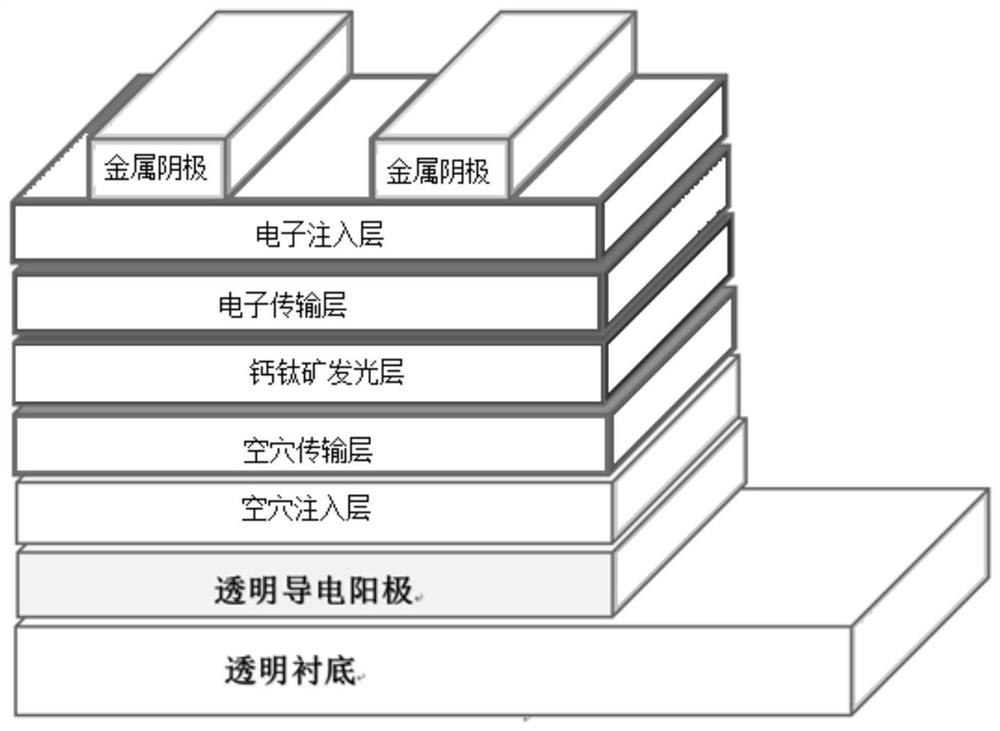
technical field [0001] The invention belongs to the technical field of perovskite light-emitting diode devices, in particular to a Ba-based 2+ Doped double cation structure red-emitting quasi-two-dimensional perovskite light-emitting diodes. Background technique [0002] Halide perovskite has become a promising light-emitting material in the field of light-emitting diodes (LEDs) due to its tunable band gap, high color purity, and low-cost and easy-to-achieve solution processing characteristics. According to the dimensions of perovskite materials, perovskites used in perovskite light-emitting diodes (PeLEDs) are mainly classified into three-dimensional perovskites, pure two-dimensional perovskites, and quasi-two-dimensional perovskites. Three-dimensional perovskites (such as MAPbI 3 ) films usually have various nonradiative recombination channels caused by defects or pinholes, which severely limit the device performance. Compared with 3D perovskite, 2D perovskite (similar ...
Claims
Login to View More Application Information
Patent Timeline
 IPC IPC(8): H01L51/50H01L51/54H01L51/56
CPCH10K71/12H10K71/40H10K85/60H10K50/11H10K71/00
Inventor康博南庞裕张子召
OwnerJILIN UNIV