Semiconductor device and mounting structure thereof

A technology of semiconductor and structure, which is applied in semiconductor/solid-state device manufacturing, semiconductor devices, semiconductor/solid-state device components, etc., can solve the problems of difficult expansion of pads for heat dissipation pads and expansion of heat dissipation area on the surface of wiring substrates, etc. To achieve the effect of ensuring the cooling area

Pending Publication Date: 2020-12-22
ROHM CO LTD
View PDF5 Cites 0 Cited by
  • Summary
  • Abstract
  • Description
  • Claims
  • Application Information

AI Technical Summary

Problems solved by technology

Therefore, it is difficult to extend the land for the heat dissipation pad on the surface of the wiring board, or to provide wiring connected to the land for the heat dissipation pad from between the lands for the electrode pad surrounding the land for the heat dissipation pad.
That is, there are cases where it is difficult to expand the heat dissipation area on the surface of the wiring substrate, resulting in the inability to secure a sufficient heat dissipation area on the surface of the wiring substrate.

Method used


Image

  • Semiconductor device and mounting structure thereof
  • Semiconductor device and mounting structure thereof
  • Semiconductor device and mounting structure thereof

Examples


no. 1 Embodiment approach

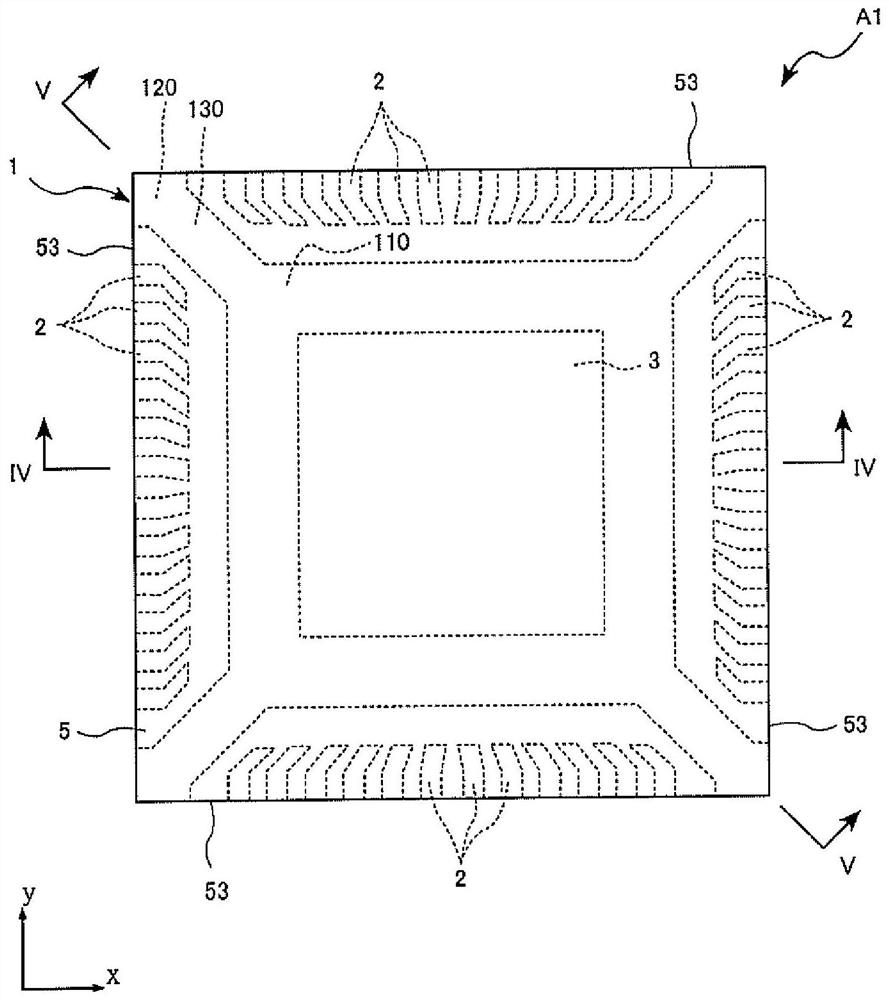
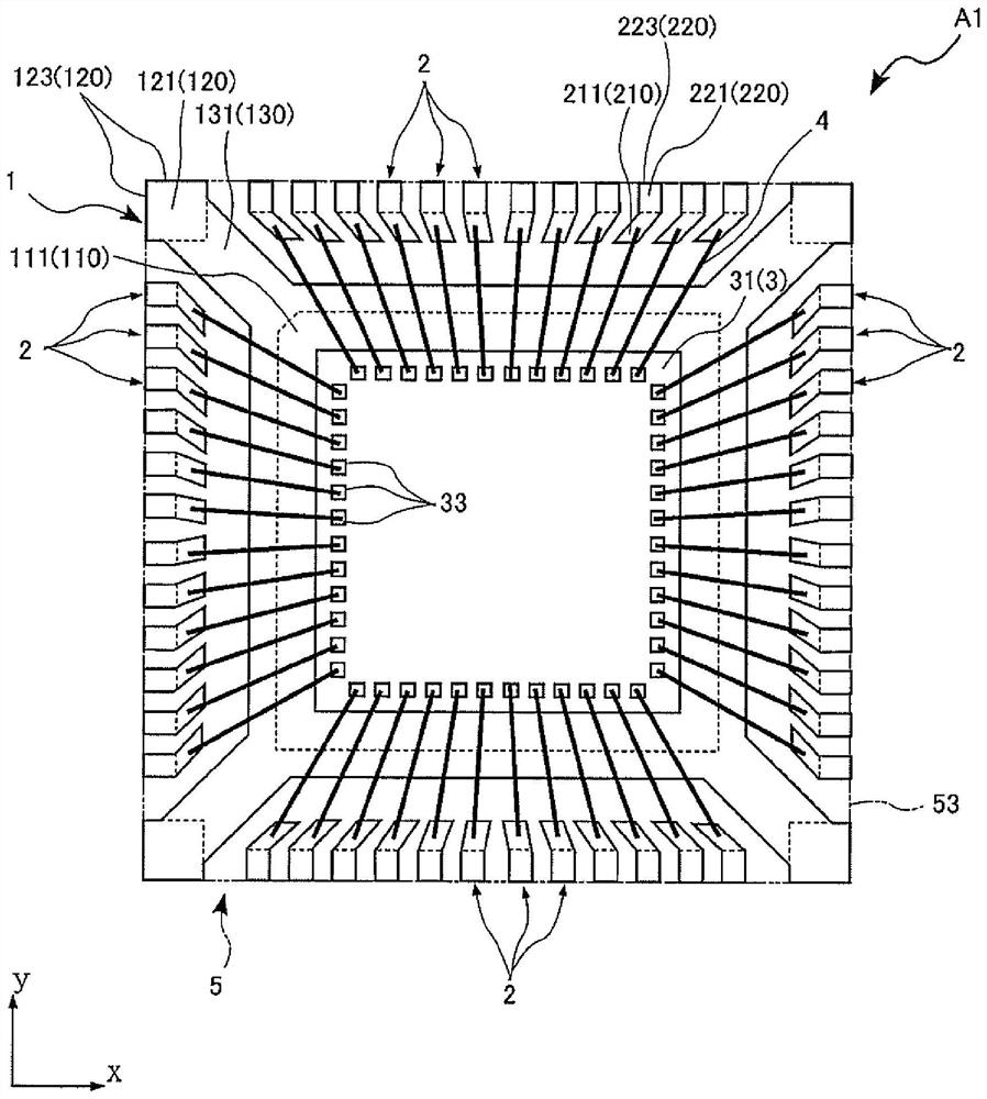
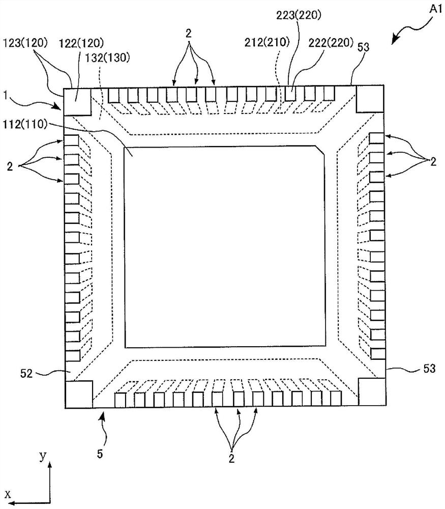
[0034] based on Figure 1 to Figure 6 The semiconductor device A1 according to the first embodiment of the present invention will be described. The semiconductor device A1 includes a first lead 1 , a second lead 2 , a semiconductor element 3 , a bonding wire 4 , and a sealing resin 5 . The semiconductor device A1 is a so-called QFN (Quad Flat Non-leaded package) package.

[0035] figure 1 It is a top view showing the semiconductor device A1. figure 2 It is a plan view showing main parts of the semiconductor device A1. image 3 It is a bottom view showing the semiconductor device A1. Figure 4 is along figure 1 Sectional view of line IV-IV. Figure 5 is along figure 1 Sectional view of the V-V line. Image 6 It is an enlarged plan view of the main part. exist figure 2 and Image 6 In FIG. 2 , for easy understanding, the outer shape of the sealing resin 5 is shown by a phantom line (dash-two dotted line) passing through the sealing resin 5 .

[0036] The semicon...

no. 2 Embodiment approach

[0077] based on Figure 13 and Figure 14 , the semiconductor device A2 according to the second embodiment of the present invention will be described. In these figures, the same reference numerals are assigned to the same or similar elements as those of the semiconductor device A1 described above, and repeated explanations will be omitted.

[0078] Figure 13 It is a bottom view showing the semiconductor device A2, and is the same as that in the first embodiment. image 3 corresponding figure. Figure 14 It is an enlarged sectional view of main parts showing a state in which the semiconductor device A2 is mounted on the wiring board 9, and is the same as that in the first embodiment. Figure 8 corresponding figure.

[0079] The semiconductor device A2 of this embodiment differs from the semiconductor device A1 in that the mounting portion back surface 112 is not exposed from the sealing resin 5 . The thickness (dimension in the z direction) of the mounting portion 110 in...

no. 3 Embodiment approach

[0082] based on Figure 15 and Figure 16 , the semiconductor device A3 according to the third embodiment of the present invention will be described. In these figures, the same reference numerals are assigned to the same or similar elements as those of the semiconductor device A1 described above, and repeated explanations will be omitted.

[0083] Figure 15 It is a bottom view showing the semiconductor device A3, and is the same as that in the first embodiment. image 3 corresponding figure. Figure 16 It is an enlarged cross-sectional view of main parts showing a state in which the semiconductor device A3 is mounted on the wiring board 9, and is the same as that in the first embodiment. Figure 8 corresponding figure.

[0084] The difference between the semiconductor device A3 of this embodiment and the semiconductor device A1 is that the connecting portion back surface 132 is exposed from the sealing resin 5 . The thickness (dimension in the z direction) of the connec...


PUM

PropertyMeasurementUnit
widthaaaaaaaaaa
thicknessaaaaaaaaaa

Abstract

The invention provides a semiconductor device capable of ensuring a heat dissipation area on a surface of a mounted wiring substrate, and a mounting structure of the semiconductor device. The semiconductor device (A1) is provided with a semiconductor element (3), a first pin (1), a plurality of second pins (2), and a sealing resin (5). The first pin (1) has: a mounting section (110) on which the semiconductor element (3) is mounted, the mounting part (110) having a rectangular shape when viewed in the thickness direction; four connecting parts (130) extending from four corners of the mountingpart (110); and four first terminal sections (120) connected to the tips of the connection sections (130), respectively. A portion of each of the first terminal portions (120) is exposed from the sealing resin (5). When the second pins (2) are observed along the thickness direction, a plurality of second pins (2) are arranged between the adjacent first terminal parts (120) and are respectively configured, and each second pin (2) is provided with a second terminal part (220) partially exposed out of the sealing resin (5) and a connecting part (210) extending from the second terminal part (220)to the mounting part (110). The connecting part width dimension (W1) of the connecting part (130) is greater than the connecting part width dimension (W2) of the connecting part (210) of the second pin (2) adjacent to the connecting part (130).

Description

technical field [0001] The present invention relates to a semiconductor device and a mounting structure of the semiconductor device. Background technique [0002] As a semiconductor device surface-mounted on a wiring substrate, a QFN (Quad Flat Non-leaded package) type semiconductor device has been developed. Patent Document 1 discloses an example of a QFN type semiconductor device. In the QFN type semiconductor device, a plurality of electrode pads are respectively arranged along four sides. In addition, QFN type semiconductor devices have a semiconductor device in which a heat dissipation pad for dissipating heat generated by a semiconductor element is disposed on the back surface. [0003] Figure 17 A bottom view of such a conventional semiconductor device A100 is shown. In the semiconductor device A100 , the first lead 1 on which the semiconductor element is mounted is exposed from the back surface of the sealing resin 5 . When the semiconductor device A100 is mount...

Claims


Application Information

Patent Timeline
Patent Type & Authority Applications(China)
IPC IPC(8): H01L21/48H01L23/31H01L23/495
CPCH01L21/4821H01L23/49541H01L23/49568H01L23/3107H01L23/49548H01L23/49503H01L2224/48245H01L2224/32245H01L2224/49173H01L24/48H01L2224/73265H01L2224/45147H01L2224/85455H01L2224/85447H01L2224/83447H01L2224/8546H01L2224/45124H01L2224/83455H01L2224/29099H01L2224/85444H01L2224/8346H01L2224/83444H01L2224/45144H01L2224/48247H01L2924/18301H01L2924/00014H01L2924/013H01L2924/01404H01L2924/00012H01L23/49838H01L23/49861H01L23/3121H01L24/45H01L23/49811H01L21/4825H01L21/4853
Inventor 安武一平
Owner ROHM CO LTD
Why Eureka
Try Eureka