Eureka AIR delivers breakthrough ideas for toughest innovation challenges, trusted by R&D personnel around the world.

nand flash programming method

A programming method and flash memory technology, applied in the field of NAND flash memory programming, can solve the problems of high programming voltage, long programming time, and affecting the service life of storage cells, and achieve the goals of reducing power consumption, short programming time, improving service life and programming efficiency Effect

Active Publication Date: 2021-09-17
CHINA FLASH CO LTD
View PDF8 Cites 0 Cited by
  • Summary
  • Abstract
  • Description
  • Claims
  • Application Information

AI Technical Summary

Problems solved by technology

[0006] In view of the above-mentioned shortcomings of the prior art, the purpose of the present invention is to provide a method for programming NAND flash memory, which is used to solve the problems in the prior art that the programming voltage is high, the programming time is long, and the service life of the storage unit is affected

Method used


Image

  • nand flash programming method
  • nand flash programming method
  • nand flash programming method

Examples


Embodiment Construction

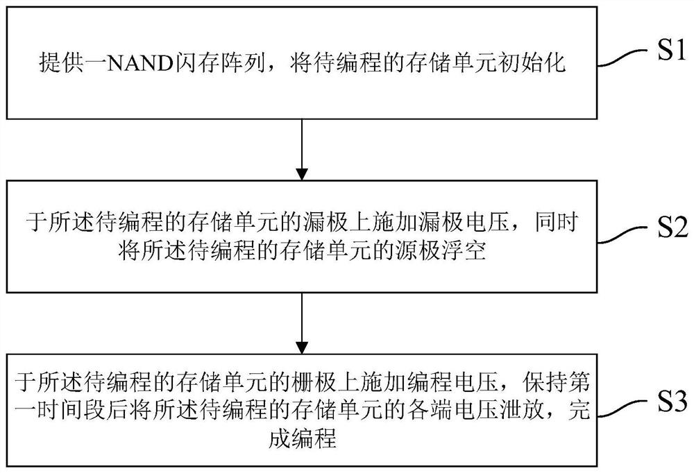
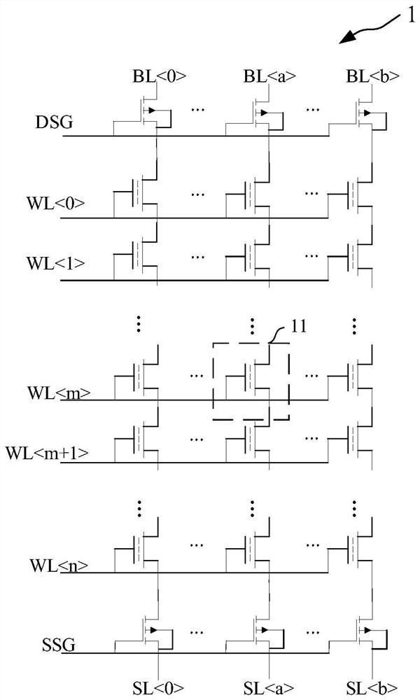
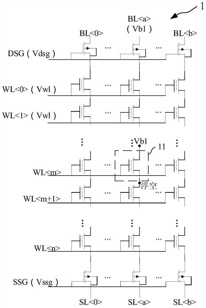
[0030] The embodiments of the present invention are described below through specific specific examples, and those skilled in the art can easily understand other advantages and effects of the present invention from the contents disclosed in this specification. The present invention can also be implemented or applied through other different specific embodiments, and various details in this specification can also be modified or changed based on different viewpoints and applications without departing from the spirit of the present invention.

[0031] see Figure 1 to Figure 4 . It should be noted that the drawings provided in this embodiment are only to illustrate the basic concept of the present invention in a schematic way, so the drawings only show the components related to the present invention rather than the number, shape and the number of components in actual implementation. For dimension drawing, the type, quantity and proportion of each component can be arbitrarily chang...


PUM


Abstract

The present invention provides a NAND flash memory programming method, comprising: providing a NAND flash memory array, initializing the storage unit to be programmed; applying a drain voltage to the drain of the storage unit to be programmed, and setting the source of the storage unit to be programmed Floating; apply a programming voltage to the gate of the memory cell to be programmed, and discharge the voltage of each terminal of the memory cell to be programmed after maintaining the first period of time to complete programming; wherein, the drain of the memory cell to be programmed and The voltage difference of the substrate is not less than 4V, the first time period is not more than 100μs, and the programming voltage is not more than 10V. After the NAND flash memory programming method of the present invention is initialized, the drain voltage is applied and the source is floated, and then the programming voltage is applied to complete the programming. The gate voltage during programming is much lower than the existing tunneling (F-N) programming method The gate voltage is high, and the programming time is short, which can effectively improve the service life and programming efficiency of the memory cell, and reduce power consumption at the same time.

Description

technical field [0001] The invention relates to the field of integrated circuit design, in particular to a NAND flash memory programming method. Background technique [0002] Flash memory refers to the most commonly used semiconductor memory that does not lose information when power is turned off. It has the advantages of small size, low power consumption, and is not susceptible to physical damage. It is an ideal storage medium for mobile digital products. The core memory of existing electronic device memory cards is flash memory. [0003] Flash memory is mainly divided into NAND type and NOR type from the array structure. NAND type is more suitable for highly integrated chips, with fast read and write speed, but cannot perform single-byte write operations, each time a data block write operation is required; while NOR type has a single-byte write operation capability, and at the same time It also supports high-speed read access, but the write operation speed is relatively ...

Claims


Application Information

Patent Timeline
Patent Type & Authority Patents(China)
IPC IPC(8): G11C16/20G11C16/34
CPCG11C16/3404G11C16/20G11C16/0483G11C16/10G11C16/08G11C16/24G11C16/32G11C16/3495G11C11/5628H10B41/30
Inventor 聂虹陈精纬
Owner CHINA FLASH CO LTD
Why Eureka
Eureka Blog
Learn More