Manufacturing method of embedded cavity and PCB

A manufacturing method and a technology for burying a cavity, which are applied in the manufacturing of printed circuits, printed circuits and electrical components connected with non-printed electrical components, etc. Simple and reliable, high alignment accuracy

Inactive Publication Date: 2021-02-19
DONGGUAN SHENGYI ELECTRONICS
View PDF5 Cites 2 Cited by
  • Summary
  • Abstract
  • Description
  • Claims
  • Application Information

AI Technical Summary

Problems solved by technology

[0006] The purpose of the present invention is to provide a method for manufacturing a built-in cavity and a PCB, which overcomes the defects in the prior art that the cavity is irregular due to glue flow

Method used


Image

  • Manufacturing method of embedded cavity and PCB
  • Manufacturing method of embedded cavity and PCB
  • Manufacturing method of embedded cavity and PCB

Examples


Embodiment 1

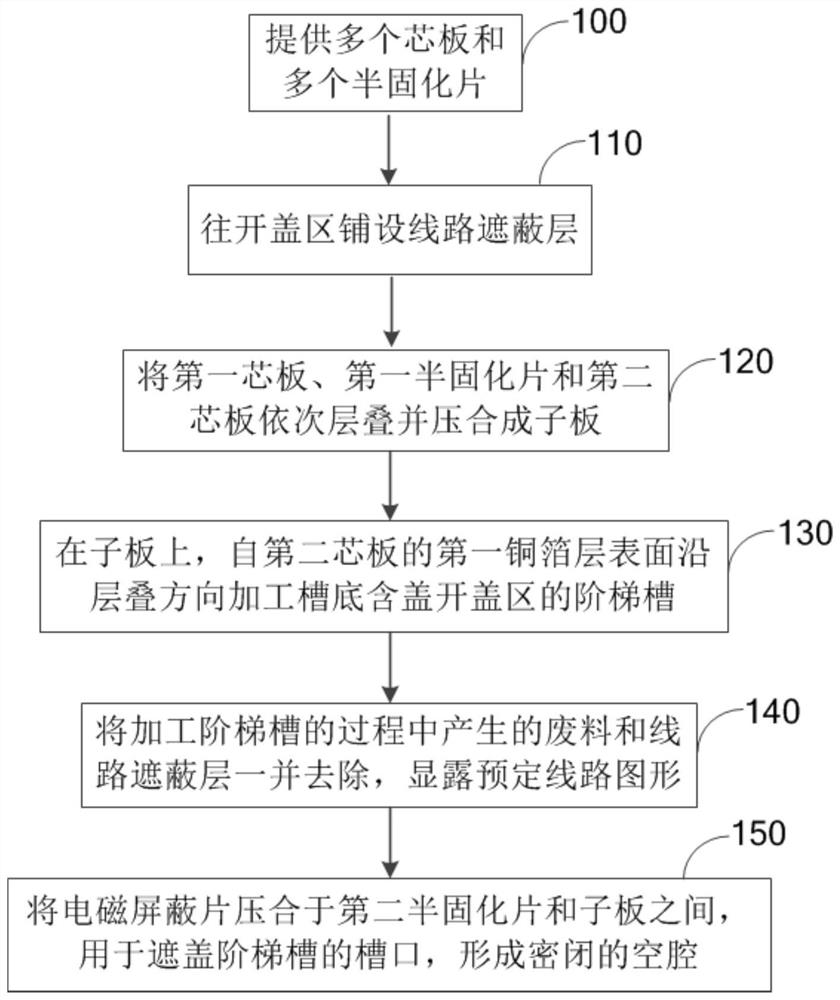
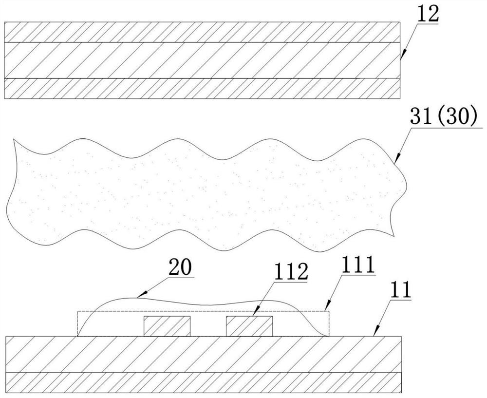
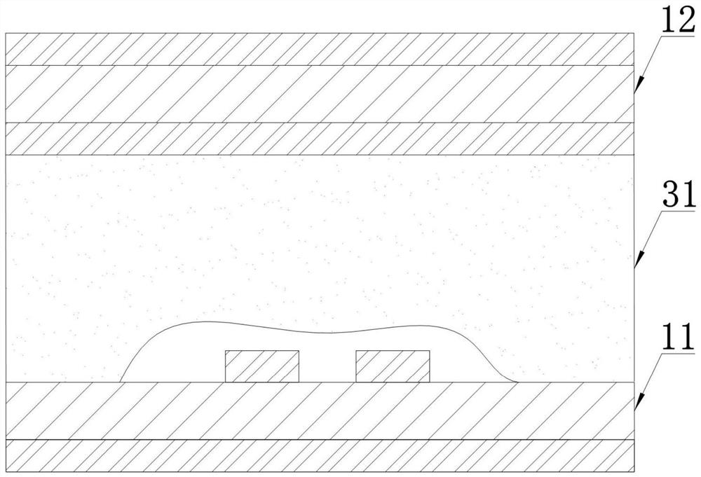
[0047] see figure 1 and figure 2 , the present embodiment provides a method for fabricating a buried cavity, comprising the steps of:

[0048] Step 100 , providing a plurality of core boards 10 and a plurality of prepregs 30 .

[0049] In this step, the core board 10 includes a first core board 11 and a second core board 12; a predetermined circuit pattern 112 is formed on the surface of the first copper foil layer of the first core board 11; the first copper foil of the first core board The surface of the layer is preset with an opening area 111. It should be noted that according to different application scenarios, the predetermined circuit pattern 112 may be partially or completely located in the opening area 111; the surface of the first copper foil layer of the first core board can also be preset. There are a plurality of opening areas 111;

[0050] The prepreg 30 includes a first prepreg 31 and a second prepreg 32 . In this embodiment, the prepreg 30 is a common prepr...

Embodiment 2

[0084] This embodiment also provides a PCB in which a closed cavity 60 is embedded, and the cavity 60 is fabricated according to the manufacturing method provided in the first embodiment.


PUM


Abstract

The invention relates to the technical field of PCBs, and discloses a manufacturing method of an embedded cavity and a PCB. The manufacturing method comprises the following steps of providing a plurality of core plates and a plurality of prepregs, laying a line shielding layer in an uncovering area, sequentially laminating a first core plate, a first prepreg and a second core plate and pressing into a daughter board, processing a stepped groove with a groove bottom containing the uncovering area, pressing an electromagnetic shielding sheet between a second prepreg and the daughter board, and covering a notch of the stepped groove, and forming a closed cavity. According to the invention, the low-fluidity prepregs are not needed, the heat-resistant reliability of the PCB is not reduced, a glue blocking pattern with higher precision requirement does not need be prepared, the manufacturing method is simpler and more reliable, the manufactured cavity is good in morphology, and the alignmentprecision of the cavity and a circuit is high.

Description

technical field [0001] The invention relates to the technical field of PCB (Printed Circuit Board, printed circuit board), and in particular, to a method for fabricating a buried cavity and a PCB. Background technique [0002] With the gradual development of the high frequency and high speed of signals in the field of communication electronics, higher requirements are put forward for the high frequency of signal lines in the PCB, the low loss transmission of high speed signals, and the impedance continuity. The design of the closed cavity can not only improve the signal transmission speed of the circuit board, but also further reduce the loss of the signal. [0003] However, it is difficult to embed the cavity inside the PCB. At present, in order to control the flow of glue and the shape of the cavity inside the closed cavity, most designs use low-fluidity prepreg for lamination, but even low-fluidity adhesive sheets are difficult to The amount of glue flow is generally mor...

Claims


Application Information

Patent Timeline
Patent Type & Authority Applications(China)
IPC IPC(8): H05K3/32H05K1/18
CPCH05K1/185H05K3/321H05K2203/1322
Inventor 吴泓宇刘梦茹肖璐
Owner DONGGUAN SHENGYI ELECTRONICS
Why Eureka
Try Eureka