Manufacturing method of embedded cavity and PCB

A manufacturing method and embedded cavity technology are applied in the directions of multilayer circuit manufacturing, printed circuit manufacturing, conductive pattern layout details, etc., which can solve problems such as irregular cavities, achieve good cavity appearance, and simple and reliable manufacturing methods , The effect of high alignment accuracy

Active Publication Date: 2021-01-22
DONGGUAN SHENGYI ELECTRONICS
View PDF6 Cites 1 Cited by
  • Summary
  • Abstract
  • Description
  • Claims
  • Application Information

AI Technical Summary

Problems solved by technology

[0006] The purpose of the present invention is to provide a method for manufacturing a built-in cavity and a PCB, which overcomes the defects in the prior art that the cavity is irregular due to glue flow

Method used


Image

  • Manufacturing method of embedded cavity and PCB
  • Manufacturing method of embedded cavity and PCB
  • Manufacturing method of embedded cavity and PCB

Examples


Embodiment 1

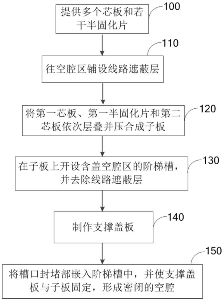
[0057] see figure 1 , figure 2 , the present embodiment provides a method for manufacturing an embedded cavity, comprising the steps of:

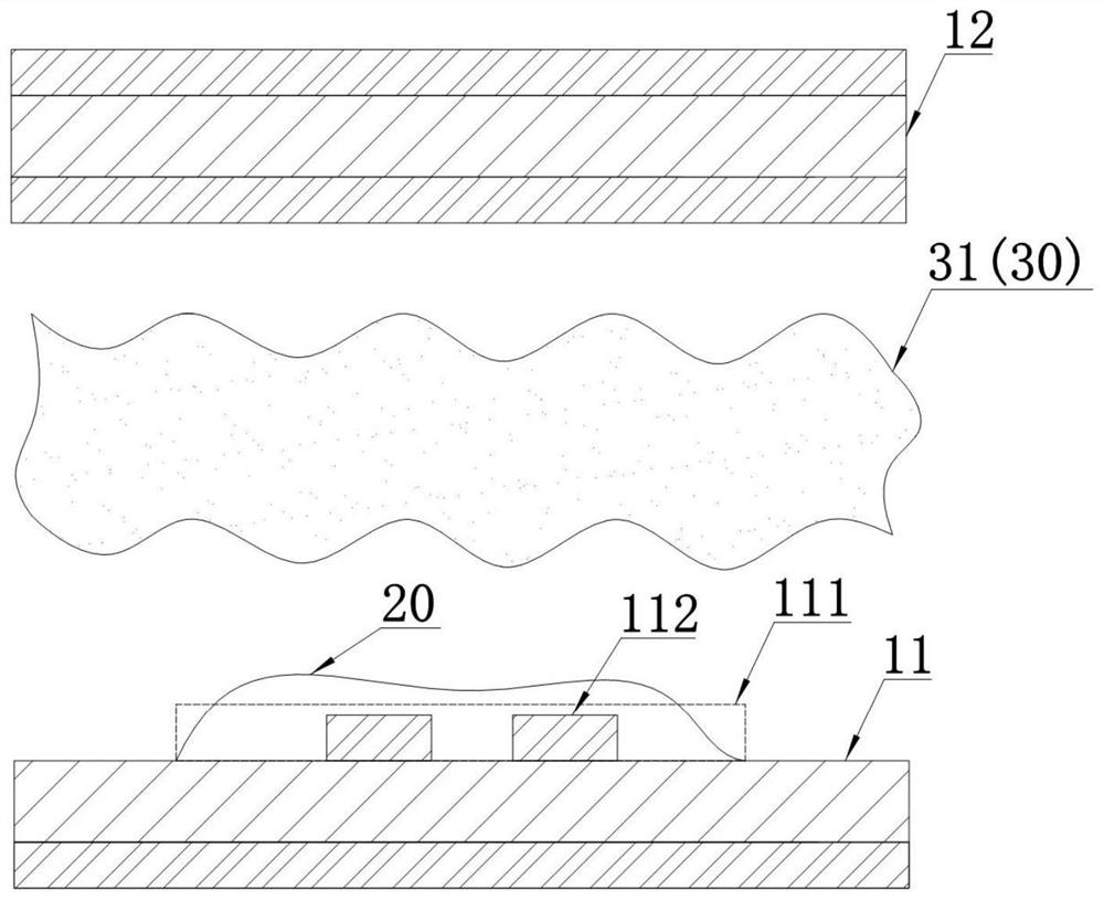
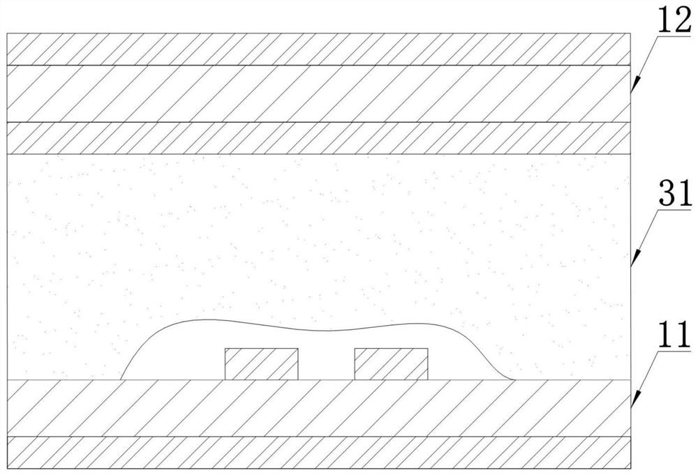
[0058] Step 100 , providing several core boards 10 and several prepregs 30 .

[0059] In this step, the core board 10 includes a first core board 11 and a second core board 12; a predetermined circuit pattern 112 is made on the surface of the first copper foil layer of the first core board 11; the prepreg 30 includes a first prepreg 31 and a second prepreg 32. In this embodiment, common prepregs are used as prepregs; the predetermined circuit pattern 112 includes high-frequency signal lines.

[0060] Wherein, the surface of the first copper foil layer of the first core board 11 is figure 2 The upper surface of the first core board 11.

[0061] Step 110 , laying the line shielding layer 20 in the cavity area 111 .

[0062] The line shielding layer 20 can use an insulating gasket, a high temperature resistant tape or an ink film, etc.,...

Embodiment 2

[0098] This embodiment also provides a PCB, in which a closed cavity 60 is embedded, and the cavity 60 is manufactured according to the manufacturing method provided in the first embodiment.

[0099] It should be noted that, as a specific implementation of this embodiment, the stepped groove 50 is a two-stage stepped groove, which is formed with two stepped surfaces, that is, the edge of the first stepped groove 51 and the first stepped groove 51. bottom of the groove, which is only a preferred embodiment of the present invention, it can be understood that the stepped groove 50 can also adopt a first-level stepped groove (only one step surface) or a multi-level stepped groove above the second level (with two More than one step surface), all can form a cavity 60 with good shape, therefore, all of them should be within the protection scope of the present invention.


PUM


Abstract

The invention relates to the technical field of PCBs, and discloses a manufacturing method of an embedded cavity and a PCB. The manufacturing method comprises the following steps: providing a first core plate and a second core plate, laying a line shielding layer in a cavity area, pressing the first core plate and the second core plate into a daughter board, forming a stepped groove containing thecavity area in the daughter board, removing the line shielding layer, embedding a notch blocking part into the stepped groove, and fixing a support cover plate and the daughter board to form a closedcavity. According to the invention, a low-fluidity prepreg is not needed, so that the heat-resistant reliability of the PCB is not reduced, meanwhile, the gummosis of the prepreg does not influence the morphology formation of the cavity, a glue blocking pattern with higher precision requirement does not need to be prepared, the manufacturing method is simpler and more reliable, and the prepared cavity is good in morphology.

Description

technical field [0001] The invention relates to the technical field of PCB (Printed Circuit Board, printed circuit board), in particular to a method for manufacturing an embedded cavity and a PCB. Background technique [0002] As the field of communication electronics gradually develops towards high-frequency and high-speed signals, higher requirements are put forward for high-frequency and low-loss transmission of high-speed signal lines in PCBs, and impedance continuity. At present, in addition to optimizing the layout design of PCB holes and lines, improving the signal transmission speed and reducing loss from the PCB processing technology is mainly through the use of media with lower Dk (dielectric constant) and Df (dielectric loss factor) as substrates and the use of rough However, these two directions have gradually emerged bottlenecks in the process of rapid development, and will face difficulties in 112G and future high-speed PCB applications. Since the Dk and Df of...

Claims


Application Information

Patent Timeline
Patent Type & Authority Applications(China)
IPC IPC(8): H05K3/46H05K1/02
CPCH05K1/0298H05K3/4611H05K3/4697
Inventor 刘梦茹吴泓宇肖璐纪成光
Owner DONGGUAN SHENGYI ELECTRONICS
Why Eureka
Try Eureka