Manufacturing method of embedded cavity and PCB

A manufacturing method and a technology for burying a cavity, which are applied in the manufacture of printed circuits, printed circuits and electrical components connected with non-printed electrical components, etc. The effect of large transmission and shielding area

Active Publication Date: 2021-01-12
DONGGUAN SHENGYI ELECTRONICS
View PDF7 Cites 0 Cited by
  • Summary
  • Abstract
  • Description
  • Claims
  • Application Information

AI Technical Summary

Problems solved by technology

[0004] The purpose of the present invention is to provide a method for manufacturing a built-in cavity and a PCB, which overcomes the defects in the prior art that the cavity is irregular due to glue flow

Method used


Image

  • Manufacturing method of embedded cavity and PCB
  • Manufacturing method of embedded cavity and PCB
  • Manufacturing method of embedded cavity and PCB

Examples


Embodiment 1

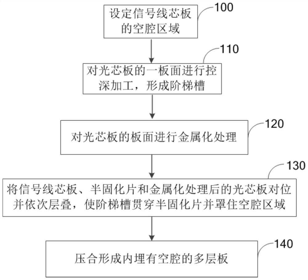
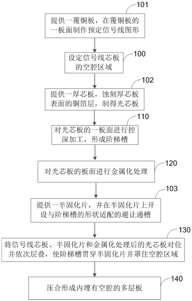
[0048] see Figure 1-Figure 7 , the present embodiment provides a method for manufacturing an embedded cavity, comprising the steps of:

[0049] Step 100 , setting the cavity area of ​​the signal line core board 30 .

[0050] In this step, the signal line core board 30 is a copper clad laminate with a predetermined signal line pattern 31 fabricated on one board surface. It should be known that the size and shape of the cavity 40 can be adjusted adaptively according to different requirements or application scenarios. In this step, setting the cavity area is used to define the desired shape and size of the cavity.

[0051] For details, please refer to Figure 6 , the cavity area is Figure 6 In the surface area of ​​the signal line core board 30 within the dotted line frame, it should be noted that, in practical applications, the predetermined signal line pattern 31 may be entirely located in the cavity area, or may be partially located in the cavity area.

[0052] Step 110 ...

Embodiment approach

[0064] As another specific implementation manner, this step specifically includes:

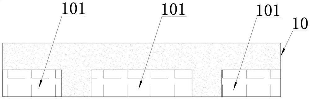
[0065] Aligning the step groove 11 and the avoidance channel 21, making the step groove 11 pass through the avoidance channel 21, and stacking the prepreg 20 on the optical core board 10;

[0066] The cavity area and the stepped groove 11 are aligned, and the signal line core board 10 is stacked on the prepreg 20 so that the cavity area is covered in the notch of the stepped groove 11 .

[0067] Step 140 , pressing to form a multi-layer board with the cavity 40 embedded therein.

[0068] The above-mentioned laminated signal line core board 30, prepreg 20, and metallized optical core board 10 are hot-pressed, and related board edge processing procedures are performed to form a multi-layer board; inside the multi-layer board, the stepped groove 11 It is in contact with the board surface of the signal line core board 30 and surrounds a cavity 40 forming a metallized cavity wall with the board su...

Embodiment 2

[0082] This embodiment also provides a PCB, in which a closed cavity 40 is embedded, and the cavity 40 is manufactured according to the manufacturing method provided in the first embodiment.

[0083] In the PCB of this embodiment, the stepped groove 11 is processed by a thick base material core board and matched with the corresponding groove on the prepreg 20, and the alignment method of the line and the cavity 40 is optimized by the alignment between the prepreg 20 and the signal line core board 30 Because the thick core board and the signal line core board 30 are directly aligned, the alignment is better, the shape of the cavity 40 is good, and the manufacturing method is simple.


PUM


Abstract

The invention relates to the technical field of PCBs, and discloses a manufacturing method of an embedded cavity and a PCB. The manufacturing method comprises the following steps of setting a cavity area of a signal line core plate, carrying out deep processing on one plate surface of an optical core plate to form a stepped groove with a groove opening capable of covering the cavity area, carryingout metallization treatment on the plate surface of the optical core plate, aligning the signal line core plate, a prepreg and the metallized optical core plate, and sequentially stacking, enabling the stepped groove to penetrate through the prepreg and cover the cavity area, and pressing to form the multilayer board with the embedded cavity. According to the present invention, the low-fluidity prepregs are not needed, the top of the cavity is not prone to collapse, the height of the cavity is constant, and it is guaranteed that impedance of a transmission line is stable; the side walls of the cavity are all made of copper, so that the anti-crosstalk performance between side-by-side signal lines is improved, the shielding area at the cavity side is increased, and transmission of high-frequency signals in the cavity is better facilitated.

Description

technical field [0001] The invention relates to the technical field of PCB (Printed Circuit Board, printed circuit board), in particular to a method for manufacturing an embedded cavity and a PCB. Background technique [0002] As the field of communication electronics gradually develops towards high-frequency and high-speed signals, higher requirements are put forward for high-frequency and low-loss transmission of high-speed signal lines in PCBs, and impedance continuity. At present, in addition to optimizing the layout design of PCB holes and lines, improving the signal transmission speed and reducing loss from the PCB processing technology is mainly through the use of media with lower Dk (dielectric constant) and Df (dielectric loss factor) as substrates and the use of rough However, these two directions have gradually emerged bottlenecks in the process of rapid development, and will face difficulties in 112G and future high-speed PCB applications. Since the Dk and Df va...

Claims


Application Information

Patent Timeline
Patent Type & Authority Applications(China)
IPC IPC(8): H05K1/18H05K3/32
CPCH05K1/185H05K3/321
Inventor 吴泓宇肖璐纪成光
Owner DONGGUAN SHENGYI ELECTRONICS
Why Eureka
Try Eureka