Manufacturing method of embedded cavity and PCB

A manufacturing method and embedded cavity technology are applied in printed circuit manufacturing, printed circuits connected with non-printed electrical components, electrical components, etc., which can solve the difficulty in operation and the design of the size and height of glue-resisting protrusions. , flow glue into the cavity and other problems, to achieve the effect of good cavity shape, simple and reliable manufacturing method, and high alignment accuracy

Active Publication Date: 2020-12-18
DONGGUAN SHENGYI ELECTRONICS
View PDF7 Cites 1 Cited by
  • Summary
  • Abstract
  • Description
  • Claims
  • Application Information

AI Technical Summary

Problems solved by technology

Compared with the low-fluidity bonding sheet, this patent solution has better reliability, but in the process of pressing the prepreg, it is difficult to design the size and height of the glue-resisting protrusion due to poor control of glue flow Accurate matching, if there is a slight error, it will cause glue to flow into the cavity. This method of preparing the cavity has a particularly high requirement for the graphic design accuracy of the resist glue, and the operation is difficult

Method used


Image

  • Manufacturing method of embedded cavity and PCB
  • Manufacturing method of embedded cavity and PCB
  • Manufacturing method of embedded cavity and PCB

Examples


Embodiment 1

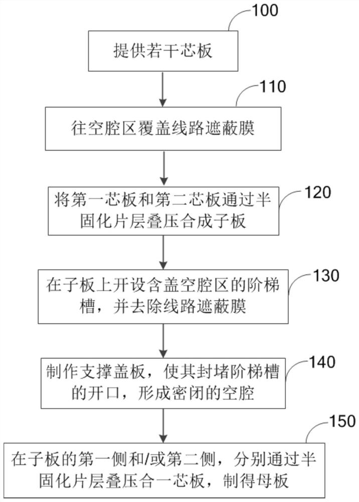
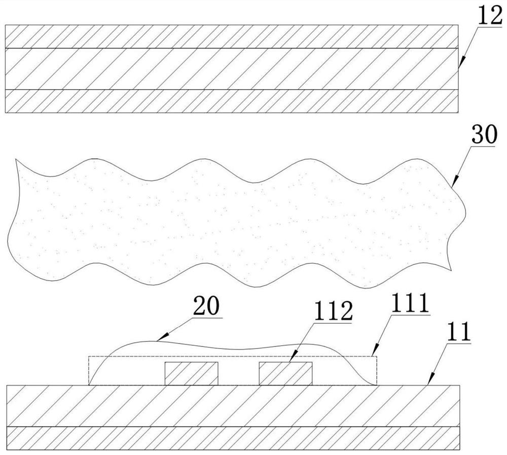
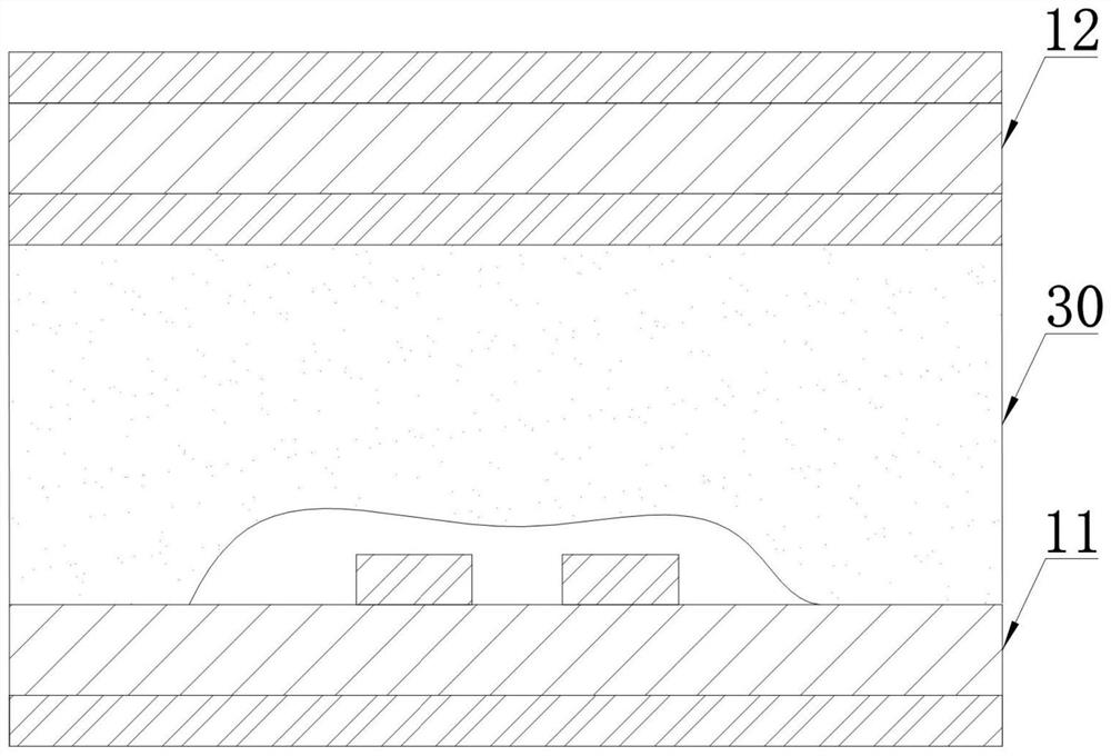
[0045] see figure 1 , figure 2 , the present embodiment provides a method for manufacturing an embedded cavity, comprising the steps of:

[0046] Step 100, providing several core boards 10;

[0047] In this step, the core board 10 includes a first core board 11 and a second core board 12; a cavity area 111 is predetermined on the surface of the first copper foil layer of the first core board 11, and a predetermined circuit pattern 112 is made in the cavity area 111 ; The predetermined line pattern 112 includes a high-frequency signal line.

[0048] Wherein, the surface of the first copper foil layer of the first core board 11 is figure 2 The upper surface of the first core board 11.

[0049] Step 110, covering the cavity area 111 with the line shielding film 20;

[0050] In this embodiment, the line shielding film 20 is a high temperature resistant adhesive tape pasted on the cavity area 111 or an ink film coated on the cavity area to cover the predetermined line patter...

Embodiment 2

[0075] This embodiment also provides a PCB, in which a closed cavity 70 is embedded, and the cavity 70 is manufactured according to the manufacturing method provided in the first embodiment.


PUM


Abstract

The invention relates to the technical field of PCBs, and discloses a manufacturing method of an embedded cavity and a PCB. The manufacturing method comprises the following steps: providing a first core plate and a second core plate, covering a cavity area of the first core plate with a line shielding film, laminating the first core plate and the second core plate into a daughter board through prepregs, forming a stepped groove covering the cavity area in the daughter board, removing the line shielding film, manufacturing a supporting cover plate to block the opening of the stepped groove, andforming a closed cavity. According to the invention, a low-fluidity prepreg is not needed, so the heat-resistant reliability of the PCB is not reduced; meanwhile, the gummosis of the prepreg does notinfluence the morphology formation of the cavity, a glue blocking pattern with higher precision requirement does not need to be prepared, the manufacturing method is simpler and more reliable, and the prepared cavity is good in morphology.

Description

technical field [0001] The invention relates to the technical field of PCB (Printed Circuit Board, printed circuit board), in particular to a method for manufacturing an embedded cavity and a PCB. Background technique [0002] With the rapid development of the information industry and the electronics industry represented by smart electronic products, digital circuits have gradually entered the stage of high-speed information processing and high-frequency signal transmission. Development in the direction of reliability and low cost; and as the field of communication electronics gradually develops in the direction of high-frequency and high-speed signals, the low-loss transmission of high-frequency and high-speed signals in PCB signal lines, impedance continuity, etc. higher requirement. Therefore, a higher and more urgent demand is put forward for the low dielectric properties of copper clad laminates; realizing PCB substrate materials with low dielectric constant (Dk) and l...

Claims


Application Information

Patent Timeline
Patent Type & Authority Applications(China)
IPC IPC(8): H05K1/18H05K3/32
CPCH05K1/185H05K3/321H05K2203/1322
Inventor 吴泓宇刘梦茹肖璐纪成光
Owner DONGGUAN SHENGYI ELECTRONICS
Why Eureka
Try Eureka