Display panel and display device

A display panel and display device technology, which is applied to the housing with display/control unit, installation of support structure, electrical equipment housing/cabinet/drawer, etc., which can solve the problem of affecting the splicing effect of the display panel, the packaging glue is not easy to level, and the equipment Problems such as high cost, to achieve the effect of reducing the wiring range, improving the binding strength, and reducing the frame

Pending Publication Date: 2021-04-02
SHENZHEN CHINA STAR OPTOELECTRONICS SEMICON DISPLAY TECH CO LTD
View PDF9 Cites 15 Cited by
  • Summary
  • Abstract
  • Description
  • Claims
  • Application Information

AI Technical Summary

Problems solved by technology

[0003] However, in the above-mentioned display device, the protection of the side printed circuit 50 and the double-sided circuit is required, the manufacturing process is complicated, the cost of related equipment is high, and precise grinding is required before the side circuit 50 is printed, which takes a long time and restricts the production capacity. After the circuit is printed, the sealing glue is not easy to level at the edge of the circuit, which affects the splicing effect of the display panel

Method used


Image

  • Display panel and display device
  • Display panel and display device
  • Display panel and display device

Examples


Embodiment Construction

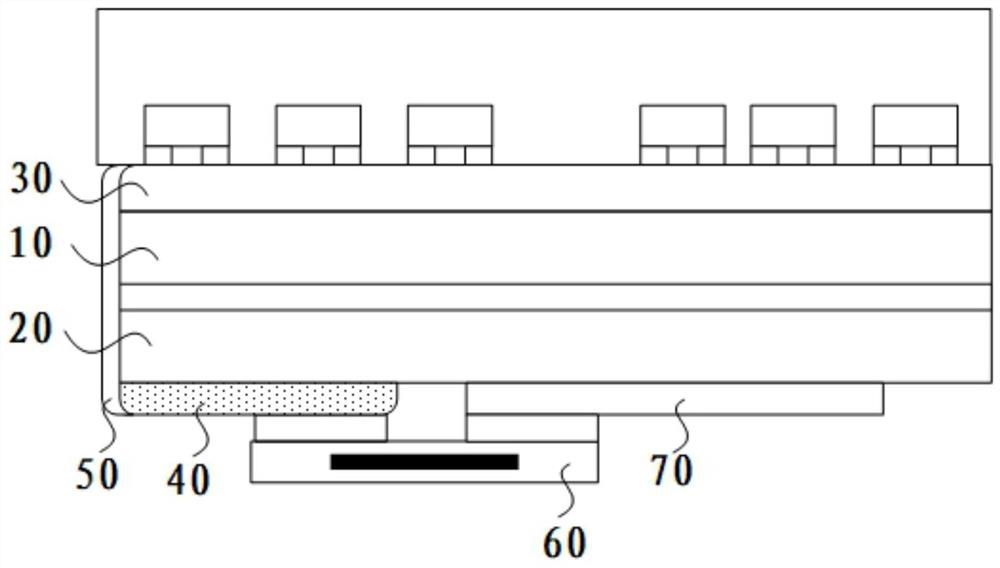
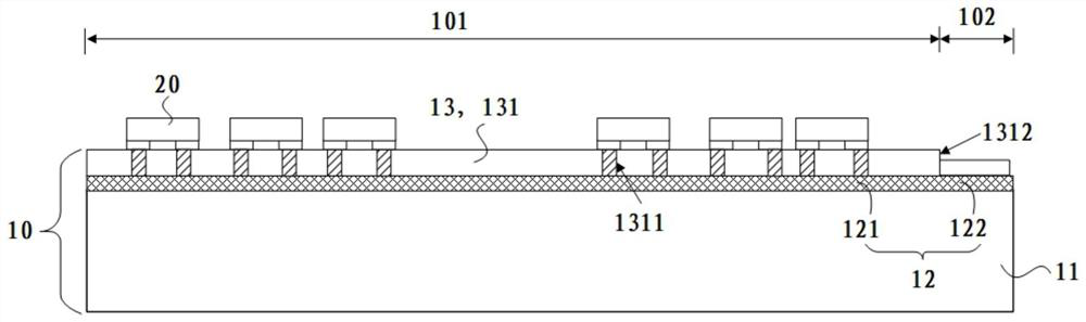
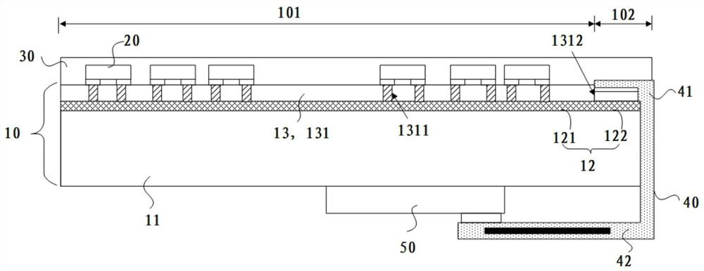
[0028] The following will clearly and completely describe the technical solutions in the embodiments of the present invention with reference to the drawings in the embodiments of the present invention. Apparently, the described embodiments are only some of the embodiments of the present invention, but not all of them. Based on the embodiments of the present invention, all other embodiments obtained by those skilled in the art without creative efforts fall within the protection scope of the present invention.

[0029] In describing the present invention, it should be understood that the terms "center", "longitudinal", "transverse", "length", "width", "thickness", "upper", "lower", "front", " Orientation indicated by rear, left, right, vertical, horizontal, top, bottom, inside, outside, clockwise, counterclockwise, etc. The positional relationship is based on the orientation or positional relationship shown in the drawings, which is only for the convenience of describing the pr...


PUM


Abstract

The invention discloses a display panel and a display device, a binding layer is arranged between a thin film transistor layer and a substrate, and a metal wire of the thin film transistor layer is electrically connected with a binding lead through a via hole, so that the range of a peripheral area can be reduced, narrow bonding can be realized, and the purpose of reducing a frame is realized.

Description

technical field [0001] The present invention relates to the field of display technology, in particular to a display panel and a display device. Background technique [0002] figure 1 Schematic diagram of the structure of the existing display device. Such as figure 1 As shown, in the existing display device, it is necessary to use the upper glass substrate 10 and the lower glass substrate 20, wherein the TFT layer 30 is provided on the upper surface of the upper glass substrate 10, and the Fanout circuit 40 is made on the lower surface of the lower glass substrate 10, so it needs to pass The side printed circuit 50 connects the TFT layer 30 with the Fanout line 40; at the same time, the chip-on-film 60 and the printed circuit board 70 are connected through the back bonding technology. [0003] However, in the above-mentioned display device, the protection of the side printed circuit 50 and the double-sided circuit is required, the manufacturing process is complicated, the ...

Claims


Application Information

Patent Timeline
Patent Type & Authority Applications(China)
IPC IPC(8): H01L27/12H01L27/15H01L27/32H05K5/00H05K5/02H05K7/14
CPCH01L27/124H01L27/156H05K5/0017H05K5/0247H05K7/14H10K59/1275H10K59/131
Inventor 樊勇
Owner SHENZHEN CHINA STAR OPTOELECTRONICS SEMICON DISPLAY TECH CO LTD
Why Eureka
Try Eureka