Array substrate and display panel

An array substrate and substrate technology, applied in semiconductor devices, electrical components, circuits, etc., can solve the problems of different display brightness, display panel mura, etc., achieve uniform distribution of electrostatic charge, improve electrostatic protection ability, and improve display uniformity. Effect

Active Publication Date: 2021-04-16
KUNSHAN GO VISIONOX OPTO ELECTRONICS CO LTD
View PDF2 Cites 1 Cited by
  • Summary
  • Abstract
  • Description
  • Claims
  • Application Information

AI Technical Summary

Problems solved by technology

Due to the difference in the accumulation of electrostatic charges in the pixel units of different columns in the display panel, the display

Method used


Image

  • Array substrate and display panel
  • Array substrate and display panel
  • Array substrate and display panel

Examples


Embodiment Construction

[0038] The present invention will be further described in detail below in conjunction with the accompanying drawings and embodiments. It should be understood that the specific embodiments described here are only used to explain the present invention, but not to limit the present invention. In addition, it should be noted that, for the convenience of description, only some structures related to the present invention are shown in the drawings but not all structures.

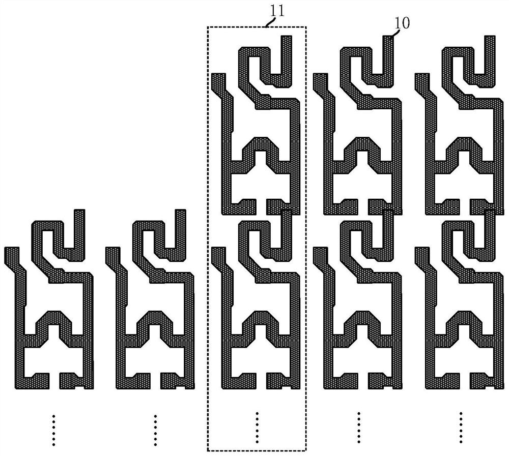
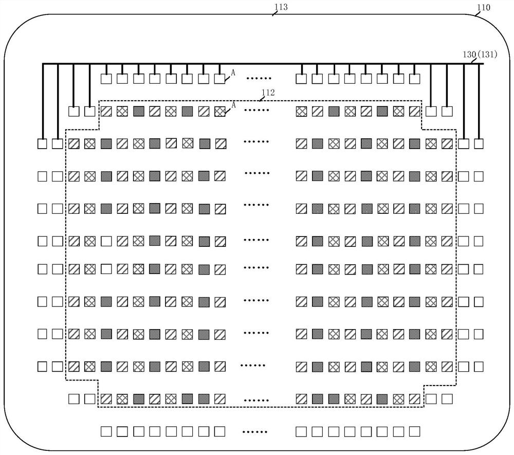
[0039] During the manufacturing process and use of the display panel, static electricity generated in the environment will accumulate and release in the display panel, causing damage to the display panel. The display panel includes pixel units in multiple rows and columns, and the pixel units include active layers for forming channels, source regions and drain regions of transistors in the pixel units. figure 1 A schematic diagram of a partial structure of an active layer of a display panel provided in the prior a...


PUM


Abstract

The invention discloses an array substrate and a display panel. The array substrate comprises a substrate, active layers and an electrically conductive layer; the active layer is arranged on the substrate, the active layers comprise a plurality of columns of patterned pixel circuit areas, each column of pixel circuit areas comprises a plurality of rows of connected pixel circuit subareas, and the pixel circuit subareas are used for forming pixel circuits; the electrically conductive layer is provided with electrically conductive wires, and the electrically conductive wires are connected with the end parts of the active layers in at least part of the pixel circuit areas, so that on the basis of not influencing the normal work of the pixel circuits, the quantity of electrostatic charges accumulated by the active layers corresponding to the pixel circuit areas in different columns can be uniformly distributed; therefore, the problem that the threshold voltage bias degrees of driving transistors formed by the active layers corresponding to different columns of pixel circuit areas are different can be solved, the electrostatic protection capability of the display panel is improved, the mura phenomenon of the display panel is improved, and the display uniformity of the display panel is improved.

Description

technical field [0001] Embodiments of the present invention relate to the field of display technologies, and in particular, to an array substrate and a display panel. Background technique [0002] In the process of manufacturing and using the display panel, there are phenomena of static electricity accumulation and static electricity discharge. Due to the difference in electrostatic charge accumulation of pixel units in different columns in the display panel, the display brightness of the pixel units in different columns of the display panel is different, resulting in a mura phenomenon in the display panel. Contents of the invention [0003] The invention provides an array substrate and a display panel to improve the antistatic ability of the array substrate and improve the uniformity of the display panel. [0004] In a first aspect, an embodiment of the present invention provides an array substrate, including: [0005] Substrate; [0006] The active layer is arranged o...

Claims


Application Information

Patent Timeline
IPC IPC(8): H01L27/12
Inventor 彭兆基张成成朱正勇马志丽朱雪婧
Owner KUNSHAN GO VISIONOX OPTO ELECTRONICS CO LTD
Why Eureka
Try Eureka