Printed circuit board and manufacturing method of printed circuit board

A technology for printed circuit boards and manufacturing methods, which is applied in the direction of printed circuit manufacturing, printed circuits, printed circuit components, etc., and can solve the problems of lack of installation and protection mechanisms, insufficient stability of circuit boards, and high manufacturing costs of circuit boards

Inactive Publication Date: 2021-04-20
SHENZHEN TONGCHUANGXIN ELECTRONICS
View PDF5 Cites 2 Cited by
  • Summary
  • Abstract
  • Description
  • Claims
  • Application Information

AI Technical Summary

Problems solved by technology

[0004] The current printed circuit board still lacks a certain installation protection mechanism in actual use, and the stability maintenance effect for the long-term use of the circuit board is insufficient, which affects its service life, and the existing me

Method used


Image

  • Printed circuit board and manufacturing method of printed circuit board
  • Printed circuit board and manufacturing method of printed circuit board
  • Printed circuit board and manufacturing method of printed circuit board

Examples


Embodiment 1

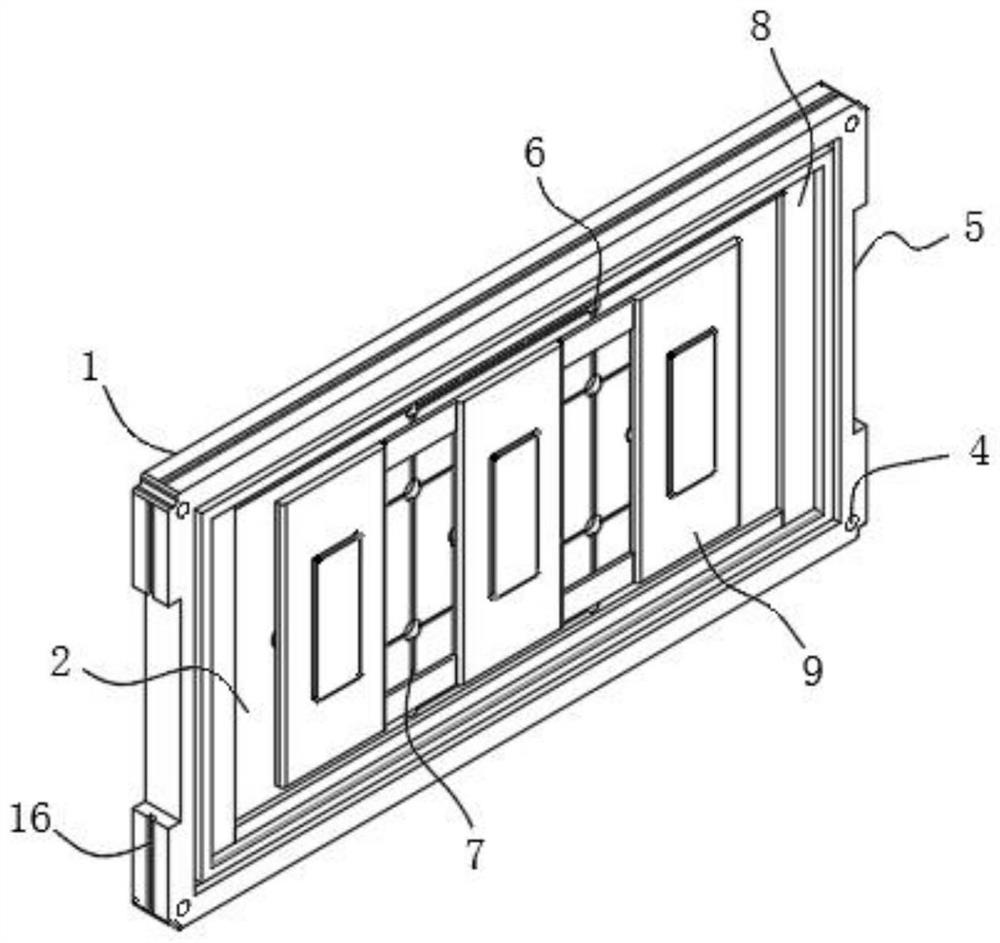
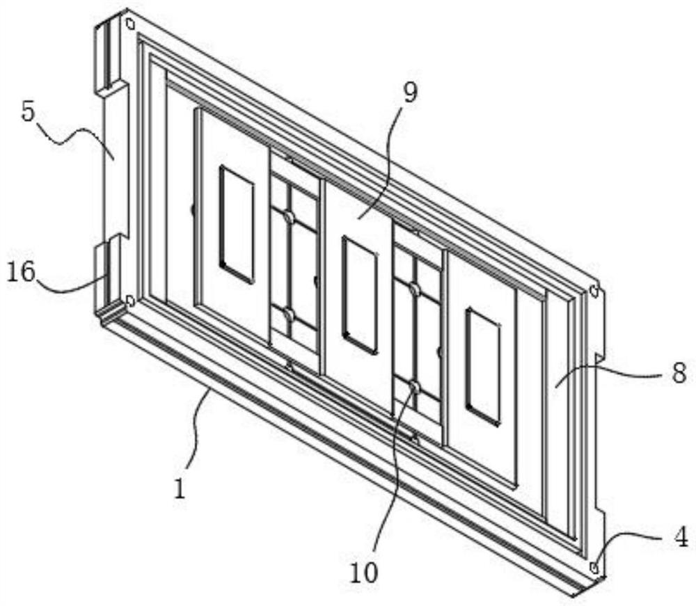
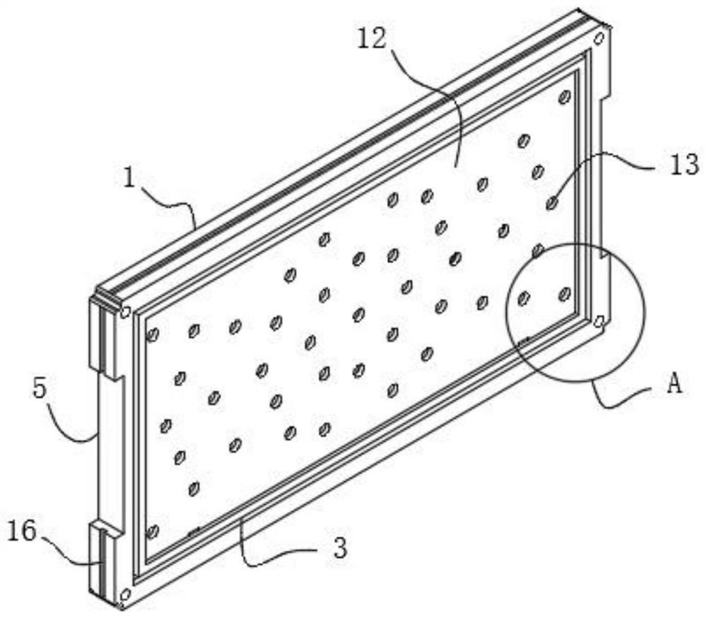
[0039] Please refer to Figure 1-6 Shown: a printed circuit board, including a substrate 1, a first mounting surface 2 and a second mounting surface 3, the two opposite surfaces of the substrate 1 are respectively provided with a first mounting surface 2 and a second mounting surface 3, which is convenient for the control module and For the construction of the protection mechanism, the core board 9 is installed on the surface of the first installation surface 2, and the surface of the first installation surface 2 is also provided with a conduction hole 10, and the inner surface of the conduction hole 10 is connected with a metal film 11, and the metal film 11 is connected with each control module. To form an electrical connection, the core board 9 is compatible with the metal film 11, which is convenient for the control module to form a control reaction effect. The side of the via hole 10 is connected with a slot-shaped hole 7, and the connection between the via hole 10 and the...

Embodiment 2

[0042] Please refer to Figure 7 Shown: a kind of manufacturing method of printed circuit board, comprises the following steps:

[0043] Step 1: Select the glass fiber board material that meets the usage standards and cut it;

[0044]Step 2: Draw the schematic diagram of the printed circuit board, and import the connection relationship and device information of the schematic diagram into the glass fiber board material;

[0045] Step 3: Process the glass fiber board material to obtain the substrate 1 of the printed circuit board, and groove the corresponding two surfaces of the substrate 1 to form two mounting surfaces;

[0046] Step 4: Lay the core board 9 and each slot hole on the first mounting surface 2 of the substrate 1 to form the required circuit connection. Specifically, each conduction hole 10 is laid with the slot-shaped hole 7 and connected to form 6 solder joints, more coherent, and maintain the use effect of printed circuit boards;

[0047] Step 5: Install prot...


PUM


Abstract

The invention discloses a printed circuit board and a manufacturing method of the printed circuit board, and relates to the technical field of printed circuit boards. The printed circuit board comprises a substrate, a first mounting surface and a second mounting surface, the two opposite surfaces of the substrate are respectively provided with the first mounting surface and the second mounting surface, the surface of the first mounting surface is provided with a core plate, a through hole is further formed in the surface of the first mounting surface, a metal film is connected with the surface of the inner side of the through hole, the core plate matches the metal film, groove-shaped holes are connected with the peripheral side of the through hole, welding spots are arranged at the connecting positions of the through hole and the groove-shaped holes, a heat dissipation plate is arranged on one side of the second mounting surface, sliding blocks are connected with the two opposite side surfaces of the heat dissipation plate, sliding grooves are formed in the surface of the inner side of the substrate, the sliding blocks match the sliding grooves in a sliding mode, and the sliding blocks are in sliding fit with the sliding grooves. The printed circuit board has an installation protection effect on a main control module, the service life of the printed circuit board can be effectively guaranteed, and the manufacturing method of the printed circuit board is simple, convenient, high in manufacturing efficiency and low in cost.

Description

technical field [0001] The invention relates to the technical field of printed circuit boards, in particular to a printed circuit board and a method for manufacturing the printed circuit board. Background technique [0002] Printed circuit boards are providers of electrical connections for electronic components. According to the number of layers of circuit boards, they can be divided into single-sided boards, double-sided boards, four-layer boards, six-layer boards and other multi-layer circuit boards. Since printed circuit boards are not general end products, Therefore, the definition of the name is slightly confusing. For example, the motherboard used for personal computers is called the motherboard, but not the circuit board directly. Although there are circuit boards in the motherboard, they are not the same. For another example: because there are integrated circuit parts loaded on the circuit board, the news media call it an IC board, but in fact it is not the same as a...

Claims


Application Information

Patent Timeline
IPC IPC(8): H05K1/02H05K1/18H05K3/00H05K3/34
Inventor 席海龙毛雪雯
Owner SHENZHEN TONGCHUANGXIN ELECTRONICS
Why Eureka
Try Eureka