Inert gas-based semiconductor wafer cleaning device for water marks and using method

An inert gas, cleaning device technology, applied in the direction of cleaning methods, cleaning methods and utensils using liquids, semiconductor/solid-state device manufacturing, etc., to achieve the effect of convenient single-sided independent cleaning and preventing stain residue and water marks

Active Publication Date: 2021-06-04
JIANGSU ASIA ELECTRONICS TECH CO LTD
View PDF5 Cites 0 Cited by
  • Summary
  • Abstract
  • Description
  • Claims
  • Application Information

AI Technical Summary

Problems solved by technology

[0004] The purpose of the present invention is to provide an inert gas-based anti-smear semiconductor wafer cleaning device and method of use to solve the problem of double-sided cleaning of the wafer

Method used


Image

  • Inert gas-based semiconductor wafer cleaning device for water marks and using method
  • Inert gas-based semiconductor wafer cleaning device for water marks and using method
  • Inert gas-based semiconductor wafer cleaning device for water marks and using method

Examples


Embodiment 1

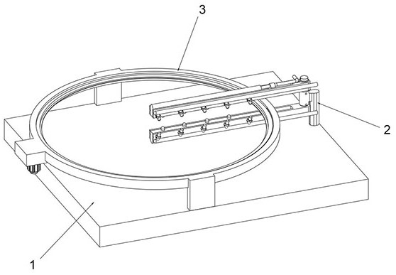
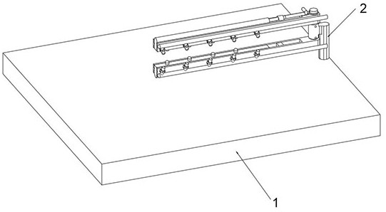
[0067] see Figure 1-Figure 15 As shown, the purpose of this embodiment is to provide a scratch-proof semiconductor wafer cleaning device based on inert gas and a method of use, including a workbench 1, a cleaning mechanism 2 and a wafer holder 3 installed on the workbench 1;

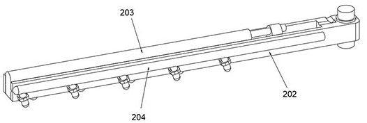
[0068] The cleaning mechanism 2 at least includes a support arm 201, the side wall of the support arm 201 is fixedly connected with a mounting seat 2011 near the top, the surface of the upper and lower ends of the mounting seat 2011 is provided with a fixing groove 2012, and the surface of the side wall of the mounting seat 2011 is provided with a The limit screw hole 2013 connected to the fixing groove 2012, the limit screw hole 2013 internal thread is connected with a lock nut, and the locking nut is pressed against the nesting rod 2051 to realize the locking of the fixing rod 205, and the two fixing grooves 2012 are both A cleaning arm 202 is fixedly installed, that is, two vertically symmetrical cle...

Embodiment 2

[0079] In order to satisfy the need for the cleaning arm to realize single-side independent rinsing of the wafer, the following improvements are made on the basis of Example 1:

[0080] see Figure 16-Figure 20 As shown, wherein, the top of the first spring 2054 is fixedly connected to the upper surface of the spring hole 20232, the lower surface of the first spring 2054 is fixedly connected to the upper surface of the mounting base 2011, the diameter of the spring hole 20232 is larger than the height adjustment hole 20231, and the first spring 2054 is nested On the outer side wall of the fixing rod 205, the side wall of the height adjustment hole 20231 is symmetrically provided with a limit card slot 2024, and the limit card block 2052 is clamped and fixed with the limit card slot 2024;

[0081] When in use, according to the need for independent flushing of one side of the wafer, twist and loosen the lock nut at the limit screw hole 2013, and rotate the cleaning arm 202 on th...

Embodiment 3

[0084] In order to meet the fine-tuning of the height of the cleaning arm during wafer rinsing, the following improvements are made on the basis of Embodiment 1:

[0085] see Figure 21 As shown, wherein, the bottom end of the fixed rod 205 is fixedly connected with a nested rod 2051, and the nested rod 2051 is clamped and fixed with the fixed groove 2012, and the nested rod 2051 can rotate in the fixed groove 2012, and the nested rod 2051 and the fixed rod 205 There is a connecting groove 2055 between them, and the connecting groove 2055 is clamped and fixed with the opening of the fixing groove 2012. The connecting groove 2055 ensures the stability of the nesting rod 2051 in the fixing groove 2012. , the top of the fixed rod 205 is threadedly connected with a compression nut 2053, the lower surface of the rotating base 2023 is provided with a spring hole 20232 communicating with the height adjustment hole 20231, and a first spring 2054 is fixedly installed in the spring hole...


PUM


Abstract

The invention relates to the technical field of wafer cleaning, in particular to a scratch-proof semiconductor wafer cleaning device based on inert gas and a use method thereof. It includes a cleaning mechanism. The cleaning mechanism includes at least a support arm. The side wall of the support arm is fixedly connected with a mounting seat near the top. There are fixing grooves on the surface of the upper and lower ends of the mounting seat. The surface of the side wall of the mounting seat is provided with a fixing groove Connected limit screw holes, the cleaning arm is fixedly installed in the two fixing grooves, one end of the cleaning arm is fixedly connected to the rotating base, the upper surface of the rotating base is provided with a height adjustment hole, and the rotating base is fixed in the mounting seat through the fixing rod. Rotation to realize the rotation adjustment of the cleaning arm, which is convenient for single-side independent cleaning of the wafer, and realizes the application of different wafer fixtures under the premise of double-sided cleaning requirements, and realizes the selection of single-sided or double-sided wafers Permanent cleaning without changing the cleaning mechanism according to the wafer holder.

Description

technical field [0001] The invention relates to the technical field of wafer cleaning, in particular to a scratch-proof semiconductor wafer cleaning device based on inert gas and a use method thereof. Background technique [0002] After the wafer is etched, it needs to be rinsed with deionized water. The traditional method is to place the wafer in the tank and rinse it through the nozzle above. After rinsing the wafer with ionized water, it is necessary to spray the surface of the wafer The inert gas is used for drying to further clean up the residues of pollutants and water stains to prevent the generation of water marks, and the centrifugal force generated by the rotation of the wafer assists the further drying of the wafer. [0003] However, the existing wafer cleaning mechanism can only clean one side of the wafer independently, and after the etching of the wafer is completed, there will be residual pollutants on both sides of the wafer. The flushing cleaning mechanism ...

Claims


Application Information

Patent Timeline
Patent Type & Authority Patents(China)
IPC IPC(8): H01L21/67H01L21/687B08B3/02B08B13/00
CPCB08B3/022B08B13/00H01L21/67051H01L21/68721H01L21/68735
Inventor 钱诚李刚童建
Owner JIANGSU ASIA ELECTRONICS TECH CO LTD
Why Eureka
Try Eureka