Wafer chip product testing and braiding equipment and processing method thereof

A technology of product testing and equipment, applied in the direction of electrical components, semiconductor/solid-state device manufacturing, circuits, etc., can solve problems such as damage, many times of chip product transfers, and low yield rate of finished products

Pending Publication Date: 2021-05-18
NORTECH AUTOMATION SHENZHEN CO LTD
View PDF0 Cites 5 Cited by
  • Summary
  • Abstract
  • Description
  • Claims
  • Application Information

AI Technical Summary

Problems solved by technology

[0004] The object of the present invention is to provide a kind of wafer chip product test taping equipment and its processing method, in order to solve the demand proposed in the above-mentioned background technology, there are many types of equipment, requiring more transfer times of chip products, longer process, each The structure of this kind of equipment is complex, and it is easy to cause problems such as dark cracks, scratches, and damage to chip products during the process. Moreover, this production method has low repeat positioning accuracy, requires multiple equipment to be used together, and the production efficiency is low. The yield rate of finished products Not high, resulting in higher actual production costs

Method used


Image

  • Wafer chip product testing and braiding equipment and processing method thereof
  • Wafer chip product testing and braiding equipment and processing method thereof
  • Wafer chip product testing and braiding equipment and processing method thereof

Examples


Embodiment Construction

[0041] The following will clearly and completely describe the technical solutions in the embodiments of the present invention with reference to the accompanying drawings in the embodiments of the present invention. Obviously, the described embodiments are only some, not all, embodiments of the present invention. Based on the embodiments of the present invention, all other embodiments obtained by persons of ordinary skill in the art without making creative efforts belong to the protection scope of the present invention.

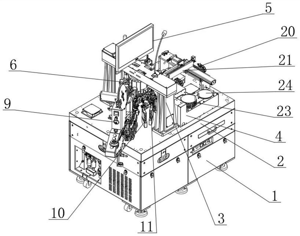
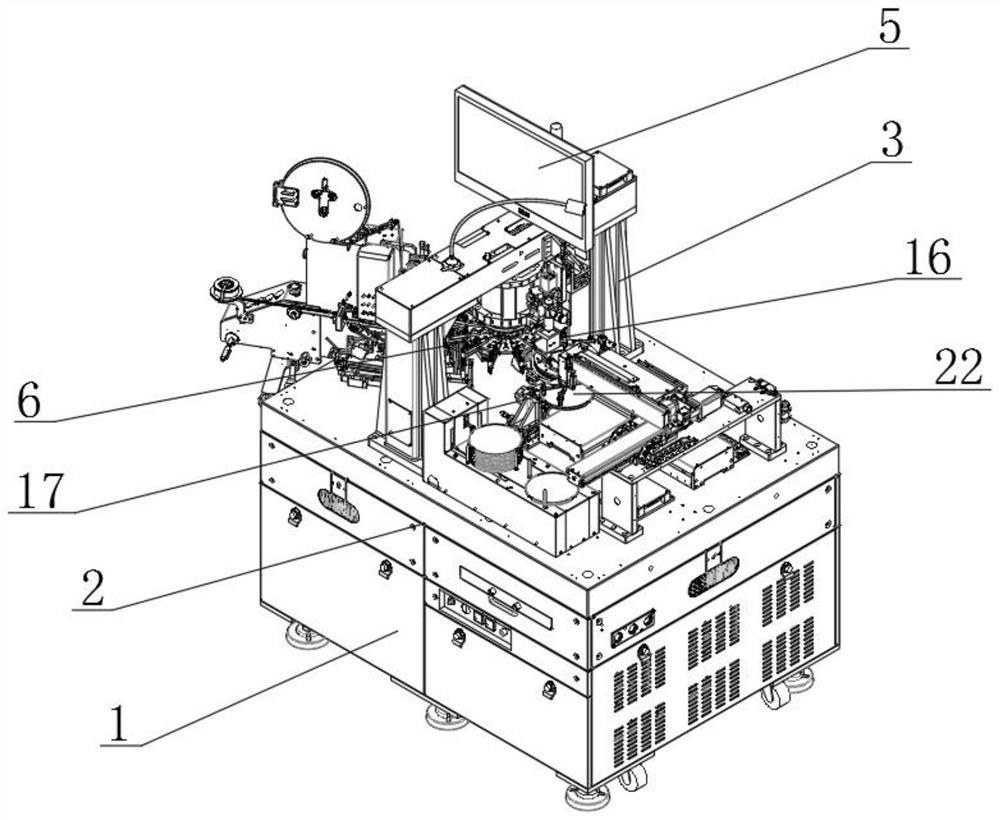
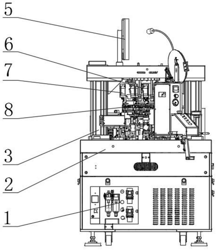
[0042] see Figure 1-3 , the present invention provides a technical solution:

[0043] A wafer chip product testing taping equipment, including an equipment electric box cabinet 1 for providing power for the entire equipment, an equipment electric box cabinet 1, electrically connected to an external power supply, and providing electric energy for the entire device, and an equipment electric box cabinet The bottom end of 1 is provided with a plurality of unive...


PUM


Abstract

The invention discloses wafer chip product testing and braiding equipment and a processing method thereof. The wafer chip product testing and braiding equipment comprises an equipment electric box cabinet used for providing power supply power for the whole equipment. The equipment electric box cabinet comprises a workbench and a gantry vertical arm mechanism, and the bottom end of the gantry vertical arm mechanism is connected to the surfaces of the two sides of the workbench through bolts, and the gantry vertical arm mechanism is used for fixing a vacuum turret module movably arranged at the bottom end of the gantry vertical arm mechanism, and the wafer disc lifting mechanism is arranged on the side, away from the gantry vertical arm mechanism, of the surface of the workbench. According to the invention, the wafer feeding system, the vacuum turret system and the chip closing processing system are reasonably arranged and formed, and through close cooperation of the wafer feeding system, the vacuum turret system and the chip closing processing system, high-speed, accurate and reliable spatial position transfer of wafer chip products can be carried out on the same equipment, rapid picking and testing of the wafer chip products from a wafer blue film are realized. The problems of dark cracks, scratches, damages and the like on wafer chip products in the process are avoided, manpower is saved, and the production efficiency is improved.

Description

technical field [0001] The invention relates to the technical field of wafer chip processing, in particular to a wafer chip product testing tape processing equipment and a processing method thereof. Background technique [0002] Wafer Level Chip Scale Packaging (WLCSP for short), that is, wafer-level chip packaging, is different from the traditional chip packaging method (cutting first and then packaging and testing, and at least 20% of the original chip is added after packaging). Volume), this latest technology is to package and test on the whole wafer first, and then cut into IC particles one by one, so the volume after packaging is equal to the original size of IC die. [0003] In the back-end production process of wafer-level chip-scale packaging products, it is necessary to pick up from the blue film of the wafer at a high speed, accurately and reliably, and perform positioning correction, electrical testing, visual inspection, and laser printing quickly and efficiently...

Claims


Application Information

Patent Timeline
Patent Type & Authority Applications(China)
IPC IPC(8): H01L21/677H01L21/683H01L21/67
CPCH01L21/67011H01L21/67271H01L21/67703H01L21/6838
Inventor 李辉王体李俊强
Owner NORTECH AUTOMATION SHENZHEN CO LTD
Why Eureka
Try Eureka