Processing method for blind slot of circuit board
A processing method and board blind technology, which is applied to printed circuit, printed circuit manufacturing, electrical components, etc., can solve the problems of processing design graphics, inability to connect circuit layers, and circuit layer circuit connections of circuit boards.
- Summary
- Abstract
- Description
- Claims
- Application Information
AI Technical Summary
Problems solved by technology
Method used
Image

Examples
Embodiment Construction
[0020] In order to make the object, technical solution and advantages of the present invention clearer, the present invention will be further described in detail below in conjunction with the accompanying drawings and embodiments. It should be understood that the specific embodiments described here are only used to explain the present invention, not to limit the present invention.
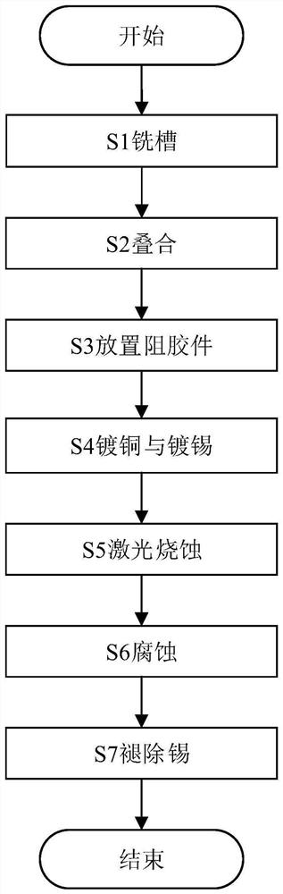
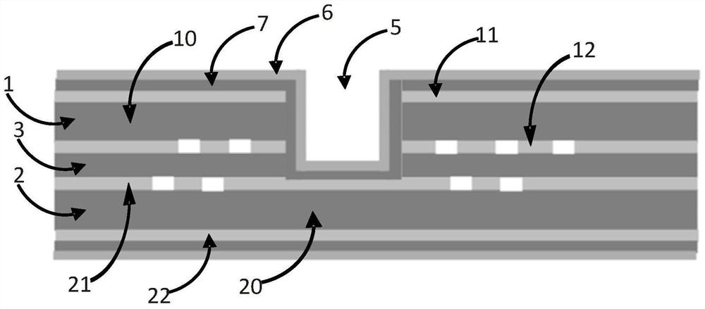
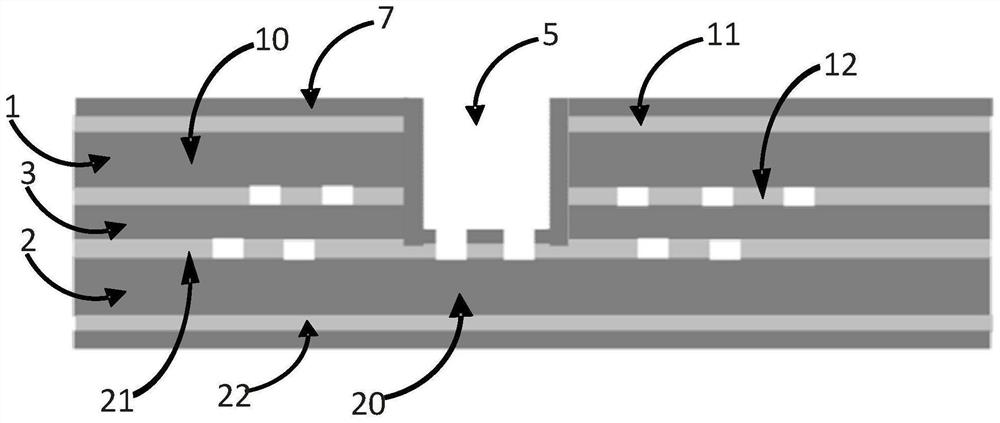
[0021] see Figure 1 to Figure 3 , the processing method for the circuit board blind slot provided by this embodiment includes:
[0022] Step S1, milling grooves on the first substrate 1 and prepreg 3 to obtain blind grooves 5;
[0023] Step S2, stacking the first substrate 1, the prepreg 3 and the second substrate 2;
[0024] Step S3, placing the glue-resisting parts in the blind slot 5 for lamination;
[0025] Step S4, taking out the glue resisting piece, and performing copper plating and tin plating in sequence;
[0026] Step S5, performing laser ablation on the tin 6 located at the bottom o...
PUM
 Abstract
Description
Claims
Application Information
 - R&D Engineer
- R&D Manager
- IP Professional
- Industry Leading Data Capabilities
- Powerful AI technology
- Patent DNA Extraction
Browse by: Latest US Patents, China's latest patents, Technical Efficacy Thesaurus, Application Domain, Technology Topic.
© 2024 PatSnap. All rights reserved.Legal|Privacy policy|Modern Slavery Act Transparency Statement|Sitemap