Perfect-absorption incident-angle-adjustable electromagnetic wave-absorbing structure
An electromagnetic absorption and perfect absorption technology, applied in the direction of electrical components, antennas, etc., can solve problems such as impedance matching
- Summary
- Abstract
- Description
- Claims
- Application Information
AI Technical Summary
Problems solved by technology
Method used
Image
Examples
Embodiment
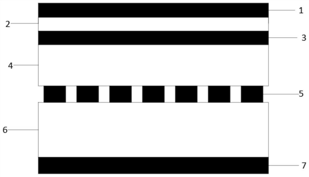
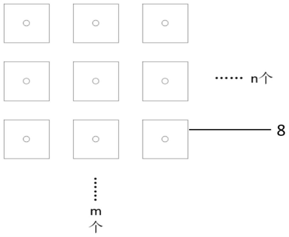
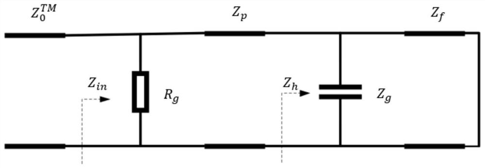
[0016] Example: such as figure 1 and figure 2 As shown, an electromagnetic wave-absorbing structure with perfect absorption and adjustable incident angles includes a first graphene layer 1, a diaphragm layer 2, a second graphene layer 3, a first dielectric substrate 4, and The first metal layer 5, the second dielectric substrate 6 and the second metal layer 7, the first graphene layer 1, the diaphragm layer 2, the second graphene layer 3, the first dielectric substrate 4, the first metal layer 5, the second The dielectric substrate 6 and the second metal layer 7 are connected to each other; the first graphene layer 1, the diaphragm layer 2, the second graphene layer 3, the first dielectric substrate 4, the second dielectric substrate 6 and the second metal layer 7 are all It is a rectangular structure, and the top view of the first graphene layer 1, the diaphragm layer 2, the second graphene layer 3, the first dielectric substrate 4, the second dielectric substrate 6 and the...
PUM
| Property | Measurement | Unit |
|---|---|---|
| length | aaaaa | aaaaa |
| radius | aaaaa | aaaaa |
Abstract
Description
Claims
Application Information


