
Electromagnetic absorption structure with optical transparency and adjustable wave absorption frequency

An optically transparent, wave-frequency technology, applied in electrical components, antennas, etc., to solve problems such as destroying the optical transparency of the overall structure

Active Publication Date: 2021-04-20
NINGBO UNIV
View PDF13 Cites 5 Cited by
  • Summary
  • Abstract
  • Description
  • Claims
  • Application Information

AI Technical Summary

Problems solved by technology

However, although the existing graphene-based electromagnetic absorption structure has optical transparency, it can only realize the adjustment of the absorption amplitude by adjusting the surface resistance of graphene. If the adjustment of the absorption frequency is to be achieved, it is still necessary to combine graphene and tunable active frequency selective surface, which would destroy the optical transparency of the monolithic structure

Method used


Image

  • Electromagnetic absorption structure with optical transparency and adjustable wave absorption frequency
  • Electromagnetic absorption structure with optical transparency and adjustable wave absorption frequency
  • Electromagnetic absorption structure with optical transparency and adjustable wave absorption frequency

Examples


Embodiment

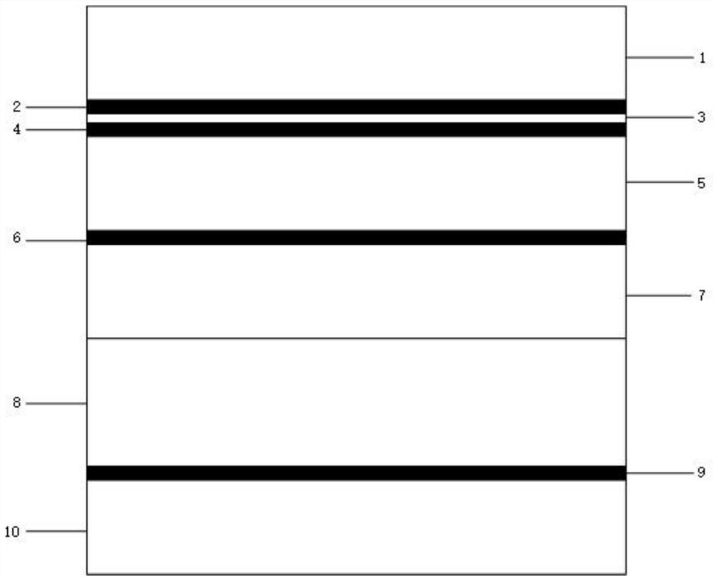
[0018] Example: such as figure 1 As shown, an electromagnetic absorption structure with both optical transparency and adjustable absorption frequency includes a first dielectric substrate 1, a first graphene layer 2, a diaphragm layer 3, and a second graphite layer stacked in sequence from top to bottom. Alkene layer 4, second dielectric substrate 5, indium tin oxide layer 6, third dielectric substrate 7, dielectric loss layer 8, reflective layer 9 and fourth dielectric substrate 10, first dielectric substrate 1, first graphene layer 2, Between the diaphragm layer 3, the second graphene layer 4, the second dielectric substrate 5, the indium tin oxide layer 6, the third dielectric substrate 7, the dielectric loss layer 8, the reflection layer 9 and the fourth dielectric substrate 10 between two adjacent layers interconnected, the first dielectric substrate 1, diaphragm layer 3, second dielectric substrate 5, third dielectric substrate 7, dielectric loss layer 8, reflective laye...


PUM

PropertyMeasurementUnit
Thicknessaaaaaaaaaa
Thicknessaaaaaaaaaa
Thicknessaaaaaaaaaa

Abstract

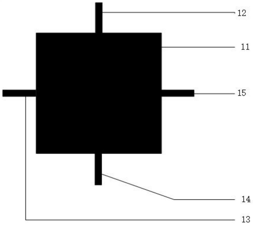
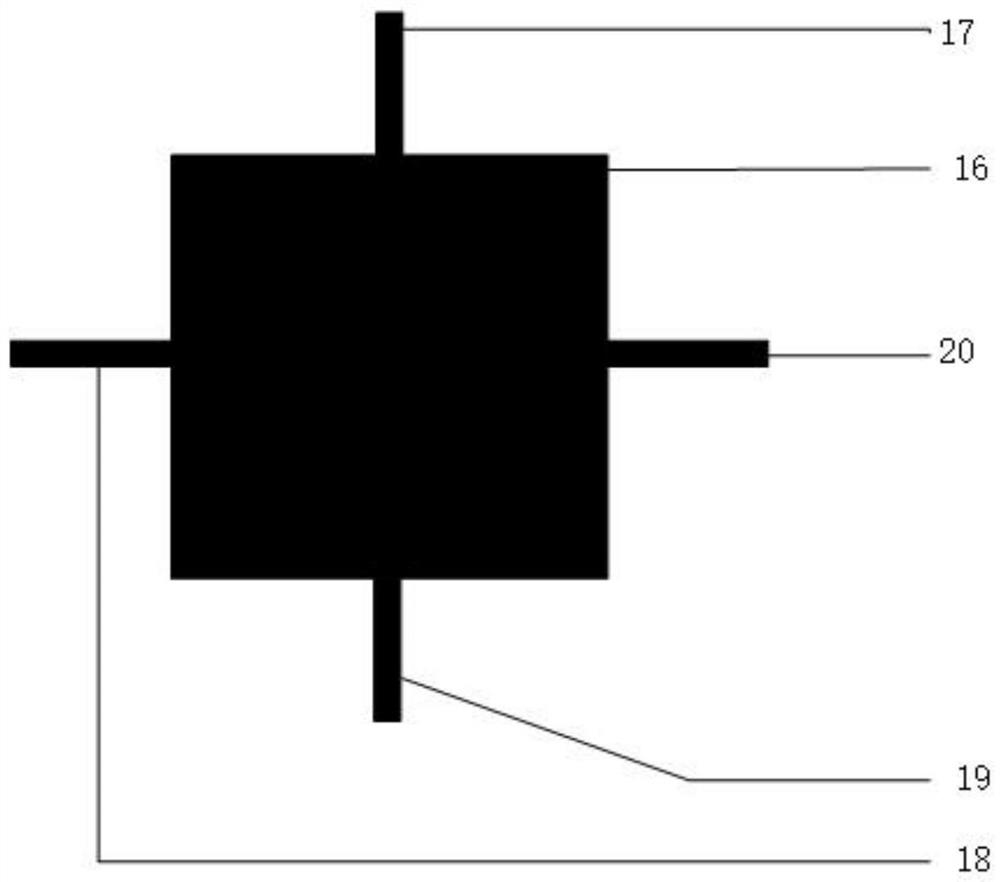
The invention discloses an electromagnetic absorption structure with optical transparency and adjustable wave absorption frequency, which comprises a first dielectric substrate, a first graphene layer, a diaphragm layer, a second graphene layer, a second dielectric substrate, an indium tin oxide layer, a third dielectric substrate, a dielectric loss layer, a reflecting layer and a fourth dielectric substrate which are stacked in sequence from top to bottom, each graphene frequency selective surface unit in the first graphene layer comprises a square graphene block and four rectangular graphene blocks distributed around the square graphene block, and the structure of the second graphene layer is completely the same as that of the first graphene layer. Each indium tin oxide frequency selective surface unit in the indium tin oxide layer comprises a square indium tin oxide block and four rectangular indium tin oxide blocks distributed around the square indium tin oxide block. The electromagnetic absorption structure has the advantages that the wave-absorbing frequency can be regulated and controlled only by regulating the resistance value of the graphene surface, and the electromagnetic absorption structure has optical transparency and also has adjustable wave-absorbing frequency in a relatively large range.

Description

technical field [0001] The invention relates to an electromagnetic absorption structure, in particular to an electromagnetic absorption structure with optical transparency and adjustable absorption frequency. Background technique [0002] As an electromagnetic stealth technology, the electromagnetic absorption structure can absorb the radar wave energy incident on the surface of the equipment, reduce the radar scattering cross-sectional area, and reduce the radar scattering characteristics of one's own target, so as to achieve low detectability. It is used in military equipment and electronic countermeasures. It is widely used in the field and plays a major role in improving the battlefield survivability of aircraft, ships, etc. [0003] In recent years, with the diversification of detection means and frequency spectrum of reconnaissance and electronic countermeasure systems, multi-spectrum and multi-functional electromagnetic stealth technology has become an urgent need to ...

Claims


Application Information

Patent Timeline
IPC IPC(8): H01Q17/00H01Q15/00
Inventor 张豫钟硕敏
Owner NINGBO UNIV
Learn More