
Optically transparent broadband electromagnetic absorption structure with adjustable wave absorption amplitude

An optically transparent, absorbing structure technology, applied in electrical components, chemical instruments and methods, synthetic resin layered products, etc., can solve the problems of inability to apply optical transparency, adjustment of the absorption amplitude, and single absorption.

Active Publication Date: 2021-07-09
NINGBO UNIV
View PDF13 Cites 4 Cited by
  • Summary
  • Abstract
  • Description
  • Claims
  • Application Information

AI Technical Summary

Problems solved by technology

[0004] The electromagnetic absorption structures with broadband absorbing frequency that have appeared at present mainly use periodic unit structures of different sizes to achieve multi-frequency point selective absorption, so as to achieve broadband absorption, such as Qihui Zhou's Multi-Frequency Broadband Terahertz Metamaterial A broadband electromagnetic absorption structure is disclosed in Absorber Based on Graphene. Although the broadband electromagnetic absorption structure has a broadband absorbing frequency, it uses opaque metal and electronic components and cannot be applied to areas that require optical transparency, such as portholes. Electromagnetic stealth in other parts, and other application fields that require optical transparency, and it cannot adjust the absorption amplitude, the absorption situation is single, and the absorption effect is general

Method used


Image

  • Optically transparent broadband electromagnetic absorption structure with adjustable wave absorption amplitude
  • Optically transparent broadband electromagnetic absorption structure with adjustable wave absorption amplitude
  • Optically transparent broadband electromagnetic absorption structure with adjustable wave absorption amplitude

Examples


Embodiment

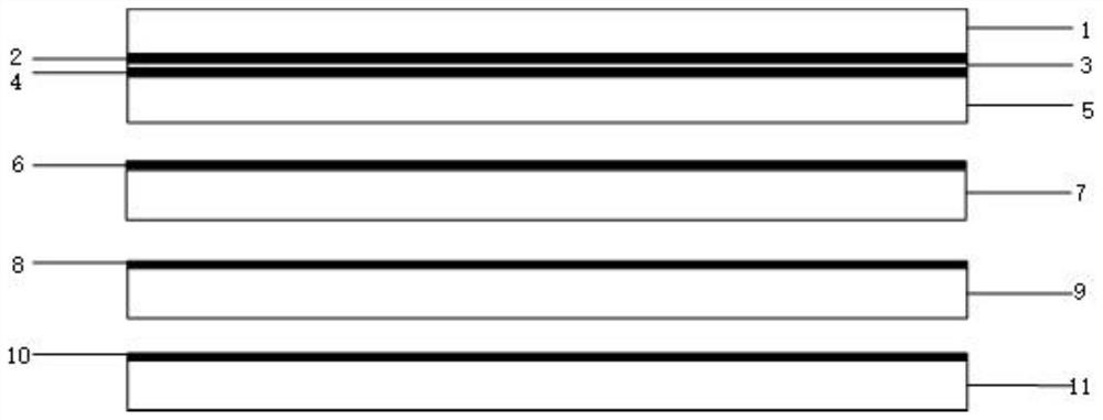
[0013] Example: figure 1 As shown, a wideband electromagnetic absorption structure having an optical transparent absorption amplitude, including the first dielectric substrate layer 1, the first stone inkyl layer 2, the diaphragm layer 3, the second graphene layer 4, the second dielectric substrate Layer 5, the first indium tin oxide layer 6, the third dielectric substrate layer 7, the second indium tin oxide layer 8, the fourth dielectric substrate layer 9, the third indium tin oxide layer 10 and the fifth medium substrate layer 11, first The dielectric substrate layer 1, the first stone insert layer 2, the diaphragm layer 3, the second graphene layer 4, the second dielectric substrate layer 5, the first indium tin oxide layer 6, the third dielectric substrate layer 7, the second indium tin oxide Layer 8, the fourth dielectric substrate layer 9, the third indium tin oxide layer 10, and the fifth medium substrate layer 11 are all rectangular, the first dielectric substrate layer 1...


PUM

PropertyMeasurementUnit
thicknessaaaaaaaaaa
thicknessaaaaaaaaaa

Abstract

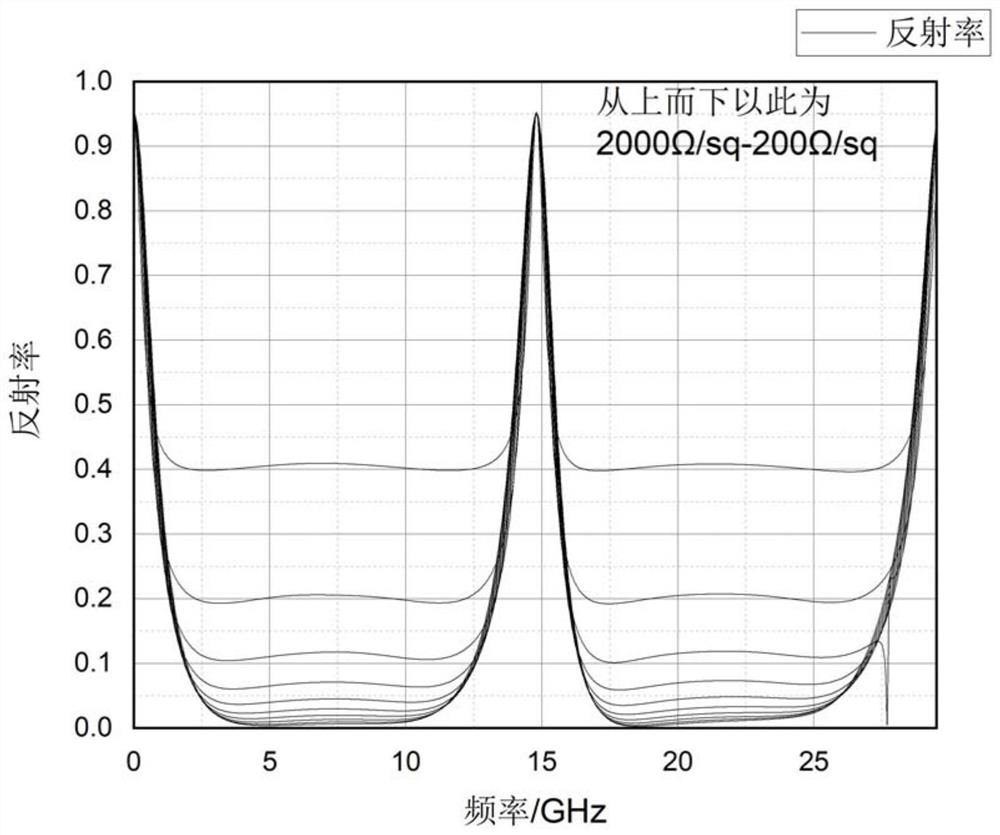
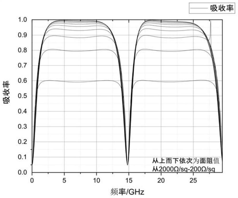
The invention discloses an optically transparent broadband electromagnetic absorption structure with an adjustable wave absorption amplitude. A first dielectric substrate layer, a first graphene layer, a diaphragm layer, a second graphene layer and a second dielectric substrate layer form a sandwich structure; and the first graphene layer and the second graphene layer have good adjustable surface resistance property and good light transmission in a microwave frequency band, the surface resistance of the first graphene layer and the second graphene layer is adjusted from 2000 ohms / sq to 200 ohms / sq by adding a bias voltage, and the wave absorbing amplitude of the whole wave absorbing structure is adjusted. The first indium tin oxide layer and the second indium tin oxide layer serve as dielectric loss layers respectively, the third indium tin oxide layer serves as a shielding reflection layer, and the third indium tin oxide layer and the sandwich structure meet the transmission theory of the transmission line together. The structure has the advantages that the wave-absorbing amplitude can be regulated and controlled by adjusting the surface resistance value of the graphene, and the wave-absorbing material has the wave-absorbing characteristics that the absorption amplitude in a large range is adjustable and the relative bandwidth is wider while the optical transparency is achieved, and the wave-absorbing effect is good.

Description

Technical field [0001] The present invention relates to a broadband electromagnetic absorption structure, and more particularly to a broadband electromagnetic absorption structure that is adjustable to an optical transparent absorption amplitude. Background technique [0002] Electromagnetic stealth technology is widely used in military equipment and electronic confrontation, which has a major role in improving the survival capacity of the battlefields such as aircraft ships. The purpose of electromagnetic stealth technology is to reduce the radar scatter characteristics of the self-objective target to achieve low-detectability of its own target. One of the main technical pathways is to use electromagnetic absorption structures with electromagnetic absorption function to absorb radar wave energy incident on the surface of the equipment. Reduce radar scattering cross-sectional area, thereby achieving stealth of radar bands. [0003] In recent years, with the exploration and electr...

Claims


Application Information

Patent Timeline
Patent Type & Authority Applications(China)
IPC IPC(8): H01Q17/00B32B27/36B32B9/00B32B9/04B32B9/06B32B29/06
CPCH01Q17/00B32B27/36B32B9/00B32B9/007B32B9/045B32B9/06B32B29/06B32B2260/028B32B2260/04B32B2307/20B32B2307/412
Inventor 张豫钟硕敏
Owner NINGBO UNIV
Learn More