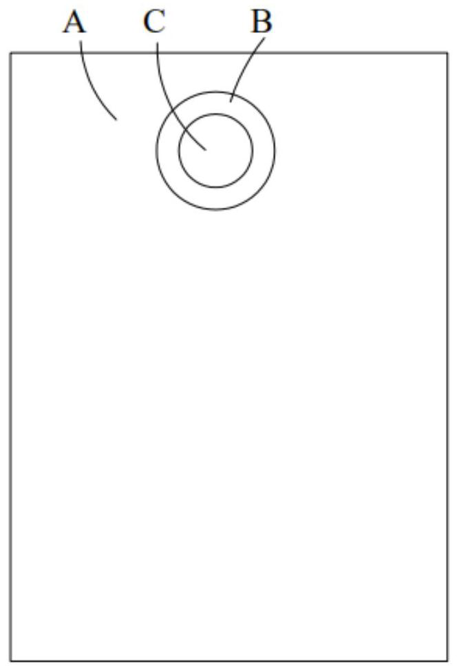
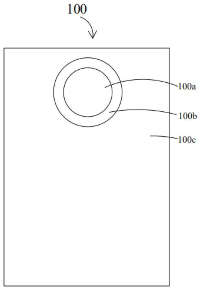
Display device

A display device and main display technology, which is applied to diodes, semiconductor devices, electrical components, etc., can solve the problem of uneven brightness in the transition display area, and achieve the effect of improving the uneven brightness and uniform reflectivity.

Active Publication Date: 2021-06-01
WUHAN CHINA STAR OPTOELECTRONICS SEMICON DISPLAY TECH CO LTD
View PDF11 Cites 3 Cited by
  • Summary
  • Abstract
  • Description
  • Claims
  • Application Information

AI Technical Summary

Problems solved by technology

[0005] The purpose of this application is to provide a display device to improve the problem of uneven brightness in the transitional display area when the display device is displayed under dark conditions

Method used


Image

  • Display device
  • Display device
  • Display device

Examples


Embodiment Construction

[0026] The technical solutions in the embodiments of the present application will be clearly and completely described below in conjunction with the drawings in the embodiments of the present application. Apparently, the described embodiments are only some of the embodiments of this application, not all of them. Based on the embodiments in this application, all other embodiments obtained by those skilled in the art without making creative efforts belong to the scope of protection of this application.

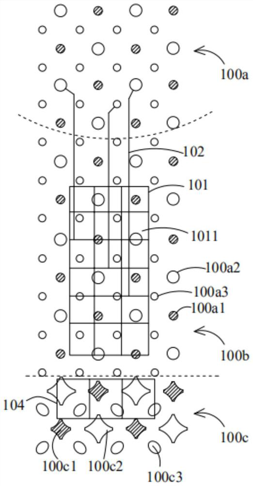
[0027] The reasons for uneven brightness in the transitional display area when displayed under dark conditions include that the metal in the transitional display area is concentrated in the area where the pixel driving circuit is located, and the area between multiple pixel driving circuits is provided with less or no metal, As a result, there is a large difference between the reflectance of the corresponding area of ​​​​the pixel driving circuit and the reflectance of the area b...


PUM


Abstract

The invention provides a display device. The display device is provided with a transition display area and a display light-transmitting area, wherein the transition display area is located on the periphery of the display light-transmitting area. The display device comprises: display pixels arranged in the transition display area and the display light-transmitting area; a plurality of pixel driving circuits, which are arranged in the transition display area and are used for driving the display pixels in the transition display area and the display light-transmitting area to emit light; and metal reflection patterns, which are arranged in the transition display area and located in gaps among the pixel driving circuits, wherein first preset metal patterns are arranged in areas corresponding to the plurality of pixel driving circuits, and the metal reflection patterns are the same as or similar to the first preset metal patterns. The metal reflection patterns at the gaps among the pixel driving circuits are the same as or similar to the first preset metal patterns in the areas corresponding to the pixel driving circuits, so the reflectivity of the transition display area tends to be uniform, and the problem that the display device is uneven in display brightness under a dark condition is solved.

Description

technical field [0001] The present application relates to the field of display technology, and in particular to a display device. Background technique [0002] like figure 1 As shown, it is a schematic diagram of a conventional organic light emitting diode display panel (Active Metrix Organic Light Emitting Diode, AMOLED). The organic light emitting diode display panel has a normal display area A, a transitional display area B and a light-transmitting display area C, and the transitional display area B is located between the light-transmitting display area C and the normal display area A. A plurality of pixel drive circuits and corresponding metal signal lines are arranged in the transition display area B. Part of the pixel drive circuits located in the transition display area B are used to drive the display pixels in the light-transmissive display area C, and the transition display area B drives the transparent The pixel drive circuits of the display pixels in the light d...

Claims


Application Information

Patent Timeline
Patent Type & Authority Applications(China)
IPC IPC(8): H01L27/32
CPCH10K59/65H10K59/12H10K59/131H10K59/121H10K50/856H10K59/1213H10K50/865
Inventor 李雪
Owner WUHAN CHINA STAR OPTOELECTRONICS SEMICON DISPLAY TECH CO LTD
Why Eureka
Try Eureka