Display device, transflective type thin film transistor array substrate and manufacture method thereof

A technology of thin film transistors and array substrates, which is applied in the field of display devices, can solve the problems of uneven brightness and poor display effect in the reflection area and transmission area, and achieve the effect of improving the display effect

Active Publication Date: 2015-01-07
BOE TECH GRP CO LTD
View PDF5 Cites 0 Cited by
  • Summary
  • Abstract
  • Description
  • Claims
  • Application Information

AI Technical Summary

Problems solved by technology

[0003] In the current process of manufacturing transflective thin film transistor liquid crystal display panels, the reflective electrodes in the array substrate and the pixel electrodes are formed together in the same patterning process. The phenomenon of uneven brightness between the transmission area and the transmission area

Method used


Image

  • Display device, transflective type thin film transistor array substrate and manufacture method thereof
  • Display device, transflective type thin film transistor array substrate and manufacture method thereof
  • Display device, transflective type thin film transistor array substrate and manufacture method thereof

Examples


Embodiment Construction

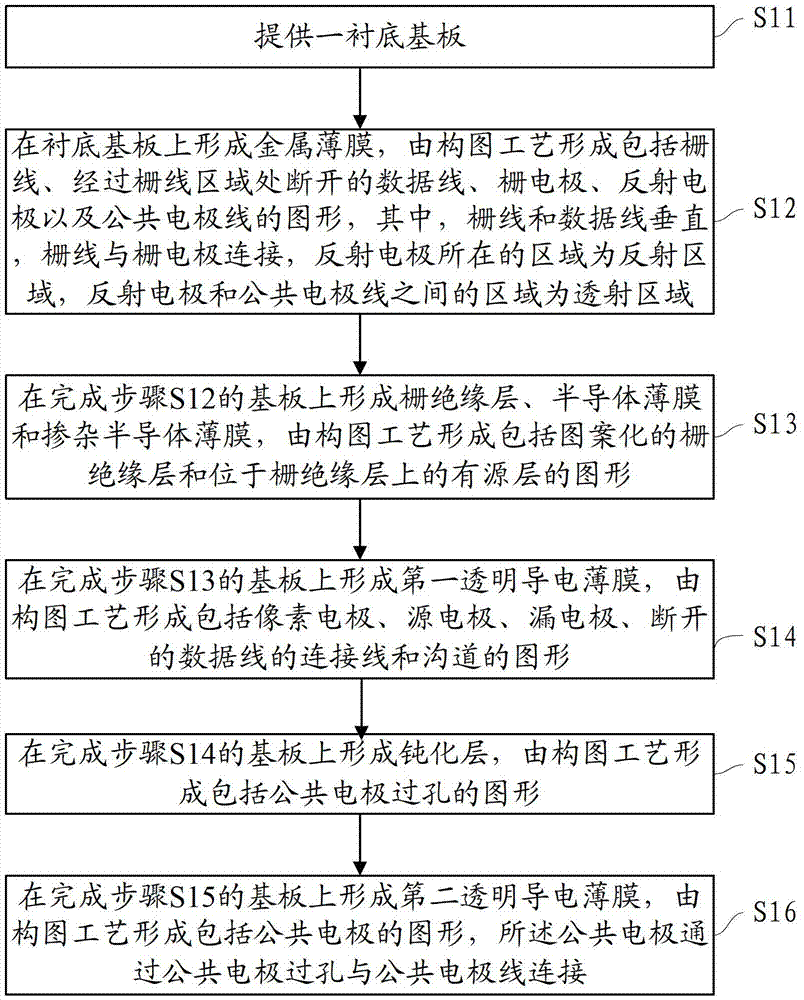
[0056] In order to make the technical problems, technical solutions and advantages to be solved by the present invention clearer, the following will describe in detail with reference to the drawings and specific embodiments.

[0057] Such as figure 1 As shown, the embodiment of the present invention provides a method for manufacturing a transflective thin film transistor array substrate, including the following steps:

[0058] S11, providing a base substrate;

[0059]S12, forming a metal thin film on the base substrate, forming a pattern including gate lines, data lines disconnected through the gate line area, gate electrodes, reflective electrodes, and common electrode lines by a patterning process, wherein the gate lines and data lines are perpendicular But do not intersect, the grid line is connected to the grid electrode, the area where the reflective electrode is located is a reflective area, and the area between the reflective electrode and the common electrode line is ...


PUM


Abstract

The present invention provides a display device, a transflective thin film transistor array substrate and a manufacturing method thereof, the manufacturing method comprises: providing a substrate; forming a gate line, a data line which is broken when passing through a gate line area, a gate electrode, a reflective electrode and a common electrode line; forming a patterned gate insulating layer and an active layer located above the gate insulating layer; forming a pixel electrode, a source electrode, a drain electrode, a connection line of the data line and a channel; forming a passivation layer and a common electrode via hole; forming a common electrode. The present invention can avoid the problem of poor display effect under strong light.

Description

technical field [0001] The invention relates to the field of display technology, in particular to a display device, a transflective thin film transistor array substrate and a manufacturing method thereof. Background technique [0002] Thin Film Transistor-Liquid Crystal Display (TFT-LCD for short) has the characteristics of small size, low power consumption, and no radiation, and occupies a dominant position in the current flat panel display market. [0003] In the current process of manufacturing transflective thin film transistor liquid crystal display panels, the reflective electrodes in the array substrate and the pixel electrodes are formed together in the same patterning process. The phenomenon of uneven brightness between the transmission area and the transmission area. Contents of the invention [0004] The technical problem to be solved by the present invention is to provide a display device, a transflective thin-film transistor array substrate and a manufacturin...

Claims


Application Information

Patent Timeline
Patent Type & Authority Patents(China)
IPC IPC(8): H01L21/84H01L27/12G02F1/1362G02F1/1368
CPCG02F1/1362G02F1/133555G02F1/134363G02F1/136286
Inventor 孔祥春刘圣烈
Owner BOE TECH GRP CO LTD
Why Eureka
Try Eureka