
White light organic light emitting diode

A light-emitting diode, organic technology, applied in the direction of electrical components, circuits, semiconductor devices, etc., can solve problems such as uneven luminance of outgoing light, easy transfer of liquid droplets to the edge, and large edge thickness of the light-emitting layer, so as to improve the luminous efficiency and improve Inhomogeneity of luminance, the effect of enhancing the action of tensile stress

Inactive Publication Date: 2018-03-13
SICHUAN JIUDINGZHIYUAN INTPROP OPERATIONS CO LTD
View PDF0 Cites 0 Cited by
  • Summary
  • Abstract
  • Description
  • Claims
  • Application Information

AI Technical Summary

Problems solved by technology

However, since the manufacturing process of the luminescent layer is mostly formed by photolithography after solution coating, when the solution is coated, the liquid droplets are easily transferred to the edge, thereby causing the edge thickness of the luminescent layer to be greater than the middle thickness. This uneven thickness will cause Luminance non-uniformity of outgoing light

Method used


Image

  • White light organic light emitting diode

Examples


Embodiment Construction

[0012] The following will clearly and completely describe the technical solutions in the embodiments of the present invention with reference to the accompanying drawings in the embodiments of the present invention. Obviously, the described embodiments are only some, not all, embodiments of the present invention. Based on the embodiments of the present invention, all other embodiments obtained by persons of ordinary skill in the art without making creative efforts belong to the protection scope of the present invention.

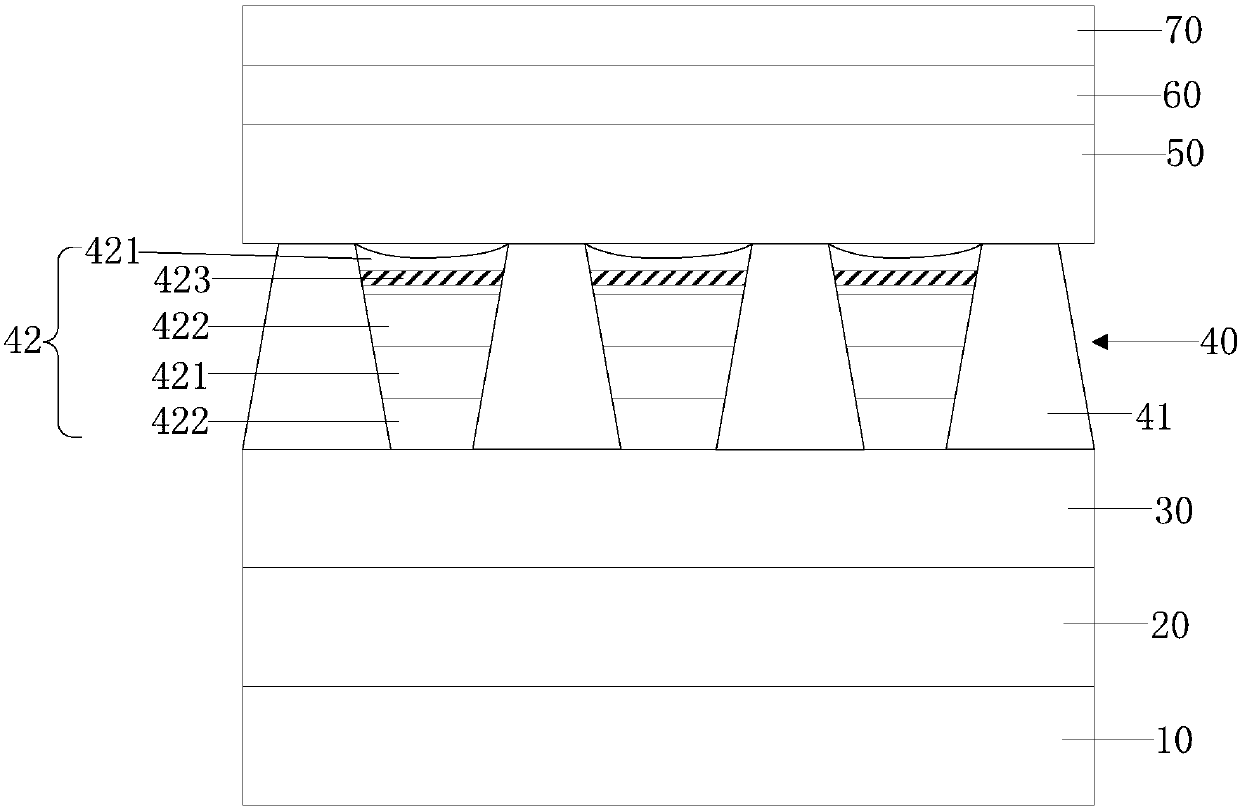
[0013] refer to figure 1 , is a schematic structural diagram of a white organic light emitting diode provided by an embodiment of the present invention. The white organic light emitting diode of this embodiment includes a silicon carbide substrate 10 , an aluminum nitride buffer layer 20 , a cathode layer 30 , an organic layer 40 , an anode layer 50 , a dielectric layer 60 and a glass panel 70 stacked in sequence.

[0014] The refractive index of the anode la...


PUM


Abstract

The invention discloses a white light organic light emitting diode. It includes a silicon carbide substrate, an aluminum nitride buffer layer, a cathode layer, an organic layer, an anode layer, a dielectric layer and a glass panel stacked in sequence. The refractive index of the anode layer is greater than that of the glass panel, and the refractive index of the dielectric layer is greater than that of the organic The refractive index of the layer, the organic layer includes an isolation layer distributed in a matrix on the cathode layer and a light-emitting layer arranged between a plurality of isolation layers, the surface of the light-emitting layer is concaved downward to form a curved surface, and the light-emitting layer is composed of a plurality of gallium nitride layers It is formed by interlacing and stacking multiple gallium nitride layers, at least one gallium nitride layer in the multiple gallium nitride layers is inserted with a stress buffer layer, and the lattice constant of the stress buffer layer is larger than that of the gallium nitride layer and the gallium nitride layer. Lattice constant of the aluminum layer. The present invention can improve the brightness unevenness of outgoing light.

Description

technical field [0001] The invention relates to the technical field of semiconductors, in particular to a white light organic light emitting diode. Background technique [0002] Most existing organic light-emitting diodes are generally composed of a cathode layer, a light-emitting layer, an anode layer and a glass layer in sequence. Electrons and holes are injected from the cathode and anode respectively, forming excitons in the light-emitting layer and exciting the material of the light-emitting layer to emit light. However, since the manufacturing process of the luminescent layer is mostly formed by photolithography after solution coating, when the solution is coated, the liquid droplets are easily transferred to the edge, thereby causing the edge thickness of the luminescent layer to be greater than the middle thickness. This uneven thickness will cause Luminance unevenness of outgoing light. Contents of the invention [0003] The main technical problem to be solved by...

Claims


Application Information

Patent Timeline
Patent Type & Authority Applications(China)
IPC IPC(8): H01L33/08H01L33/12H01L33/32
CPCH01L33/08H01L33/12H01L33/32
Inventor 罗艳
Owner SICHUAN JIUDINGZHIYUAN INTPROP OPERATIONS CO LTD
Learn More