GaN-based HEMT device and manufacturing method thereof
A manufacturing method and device technology, applied in semiconductor/solid-state device manufacturing, semiconductor devices, electrical components, etc., can solve problems such as low reliability, complex system design, and high cost, and achieve stability, cost reduction, and simplified structure Effect
- Summary
- Abstract
- Description
- Claims
- Application Information
AI Technical Summary
Problems solved by technology
Method used
Image
Examples
Embodiment 1
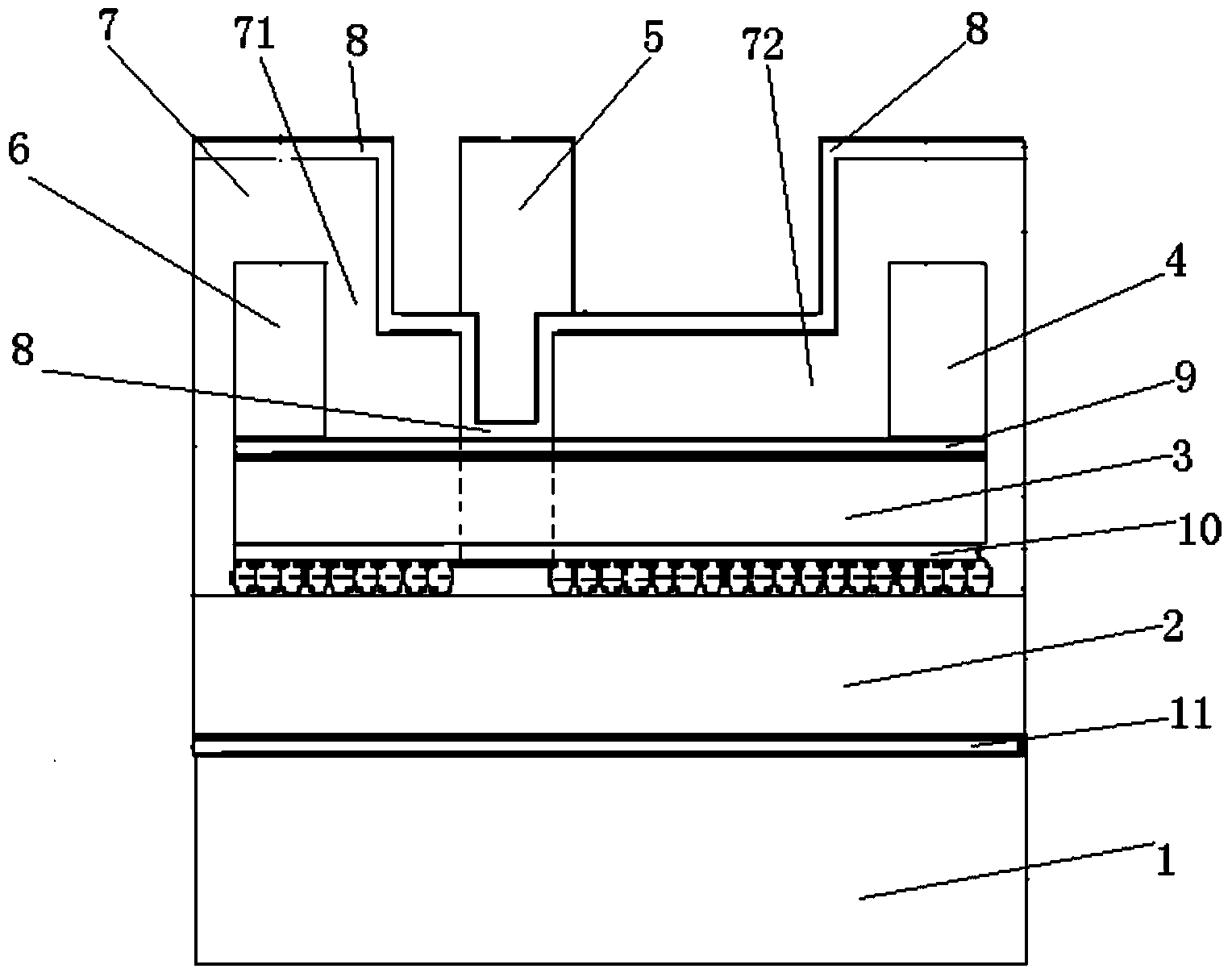
[0043] Such as figure 1 As shown, a GaN-based HEMT device provided by an embodiment of the present invention includes: a substrate 1, a GaN buffer layer 2, a barrier layer 3, a first passivation layer 7, and a second passivation layer 8. The gate 5, the source 6 and the drain 4, the substrate 1, the GaN buffer layer 2 and the barrier layer 3 are arranged sequentially from bottom to top;
[0044] The first passivation layer 7 is disposed on the barrier layer 3, the first passivation layer 7 includes a left semi-passivation layer 71 and a right semi-passivation layer 72, the left semi-passivation layer 71 is located Between the source 6 and the gate 5, the right semi-passivation layer 72 is located between the gate 5 and the drain 4;
[0045] The second passivation layer 8 is arranged on the first passivation layer 7, the two sides of the second passivation layer 8 are arranged on the first passivation layer 7, and the middle of the second passivation layer 8 Part of it is arr...
Embodiment 2
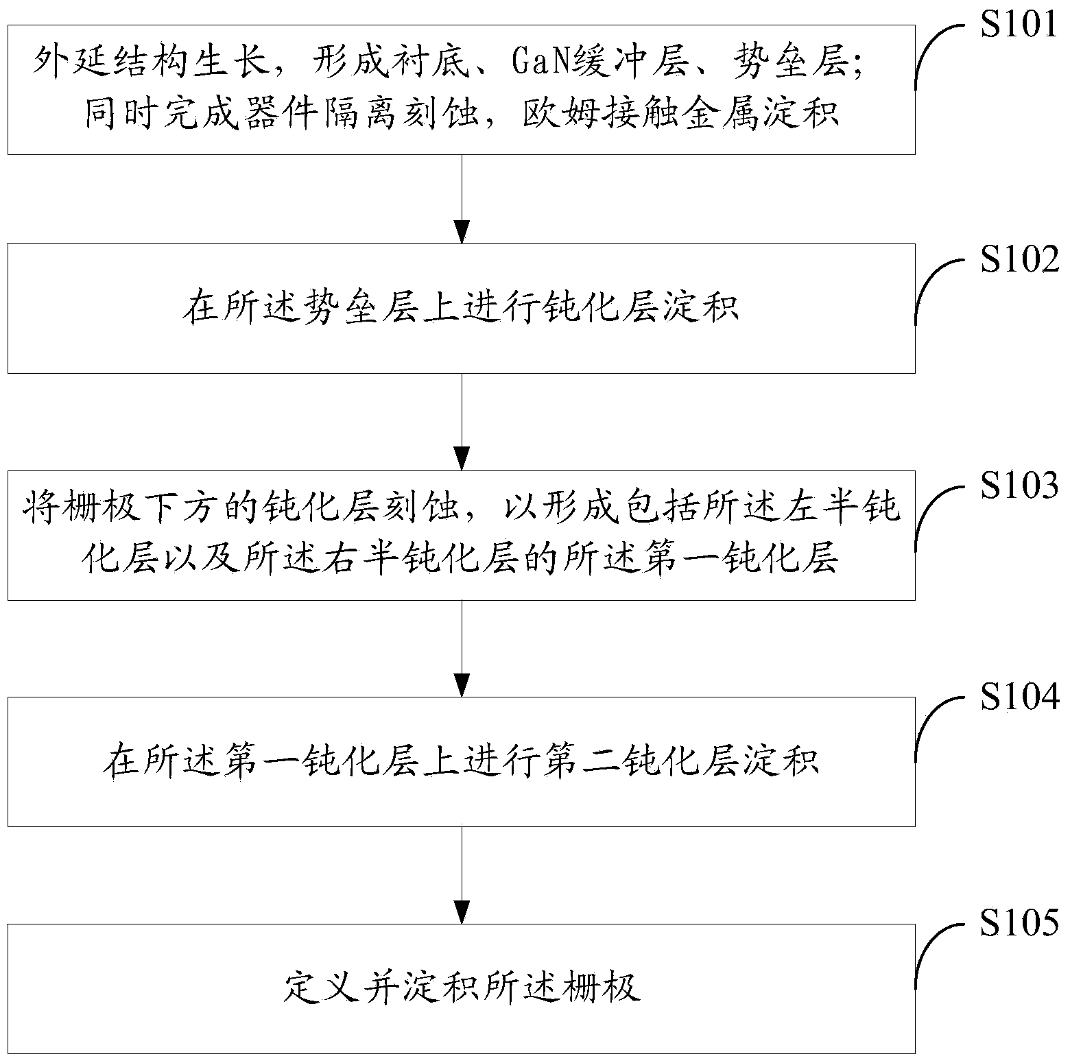
[0057] Such as figure 2 As shown, a GaN-based HEMT device fabrication method provided by an embodiment of the present invention, the fabrication method specifically includes:
[0058] S101, growing the epitaxial structure to form a substrate, a GaN buffer layer, and a barrier layer; at the same time, completing device isolation etching and ohmic contact metal deposition.
[0059] S102, depositing a passivation layer on the barrier layer; that is, depositing a first passivation layer on the barrier layer of the epitaxial structure; depositing the first passivation layer, so that the first passivation The barrier layer under the action of the GaN layer is subjected to greater tensile stress, and the surface potential of the barrier layer changes, resulting in an increase in the two-dimensional electron gas density of the GaN buffer layer. Due to the material characteristics of GaN-based materials, there are many dangling bonds on the surface, forming defect energy levels and a...
PUM
 Abstract
Description
Claims
Application Information
 - R&D
- Intellectual Property
- Life Sciences
- Materials
- Tech Scout
- Unparalleled Data Quality
- Higher Quality Content
- 60% Fewer Hallucinations
Browse by: Latest US Patents, China's latest patents, Technical Efficacy Thesaurus, Application Domain, Technology Topic, Popular Technical Reports.
© 2025 PatSnap. All rights reserved.Legal|Privacy policy|Modern Slavery Act Transparency Statement|Sitemap|About US| Contact US: help@patsnap.com


