Memory cell access device having a pn-junction with polycrystalline and single-crystal semiconductor regions

a memory cell and polycrystalline technology, applied in the direction of bulk negative resistance effect devices, solid-state devices, instruments, etc., can solve the problems of unacceptably high off-current of diodes having both regions made of doped polysilicon, difficult bipolar junction transistors with cmos peripheral circuitry, and high design and manufacturing processes. achieve the effect of enhancing the performance of the diodes, preventing the diffusion of dopants, and saving substantial manufacturing costs

Active Publication Date: 2010-05-13
MACRONIX INT CO LTD
View PDF106 Cites 134 Cited by
  • Summary
  • Abstract
  • Description
  • Claims
  • Application Information

AI Technical Summary

Benefits of technology

[0026]In some embodiments of the methods, a thin layer of a barrier material (for example SiO2 or SiNxOy) is formed on the lightly-doped region of the first conductivity type prior to depositing the polycrystalline semiconductor material; as a result a thin barrier is provided at the pn-junction. The barrier layer can inhibit diffusion of dopants across the pn-junction, and can enhance performance of the diode.
[0027]Advantageously certain features of the memory array and of peripheral devices may be formed together. For example, the deposit of polycrystalline material may constitute both the polycrystalline semiconductor node of the diode array and the FET gate in the peripheral devices. Briefly: the crystalline semiconductor material in the memory array region is doped; trench isolation are formed; an oxide is grown over the memory array region and the peripheral device region; the oxide is patterned to form gate oxides for the peripheral devices and to remove the oxide from the memory array; and polycrystalline material is deposited and patterned for both in the peripheral device region to form gates and in the array area to form polysilicon, more heavily doped elements of the access devices. Thereafter an interlayer dielectric is formed, and openings are formed in both the peripheral device region and the memory array re

Problems solved by technology

Bipolar junction transistors (BJT) can provide larger current drive than field effect transistors, but the integration of bipolar junction transistors with CMOS peripheral circuitry is difficult and results in highly complex designs and manufacturing processes.
However, diodes having both regions made of doped polysilicon may have an unacceptably high off current.
Diodes having both regions made of doped single-crystal silicon may provide a suitably low off current, but

Method used


Image

  • Memory cell access device having a pn-junction with polycrystalline and single-crystal semiconductor regions
  • Memory cell access device having a pn-junction with polycrystalline and single-crystal semiconductor regions
  • Memory cell access device having a pn-junction with polycrystalline and single-crystal semiconductor regions

Examples


Embodiment Construction

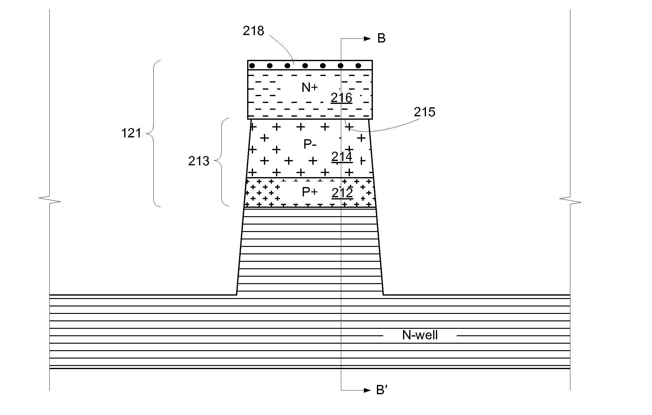
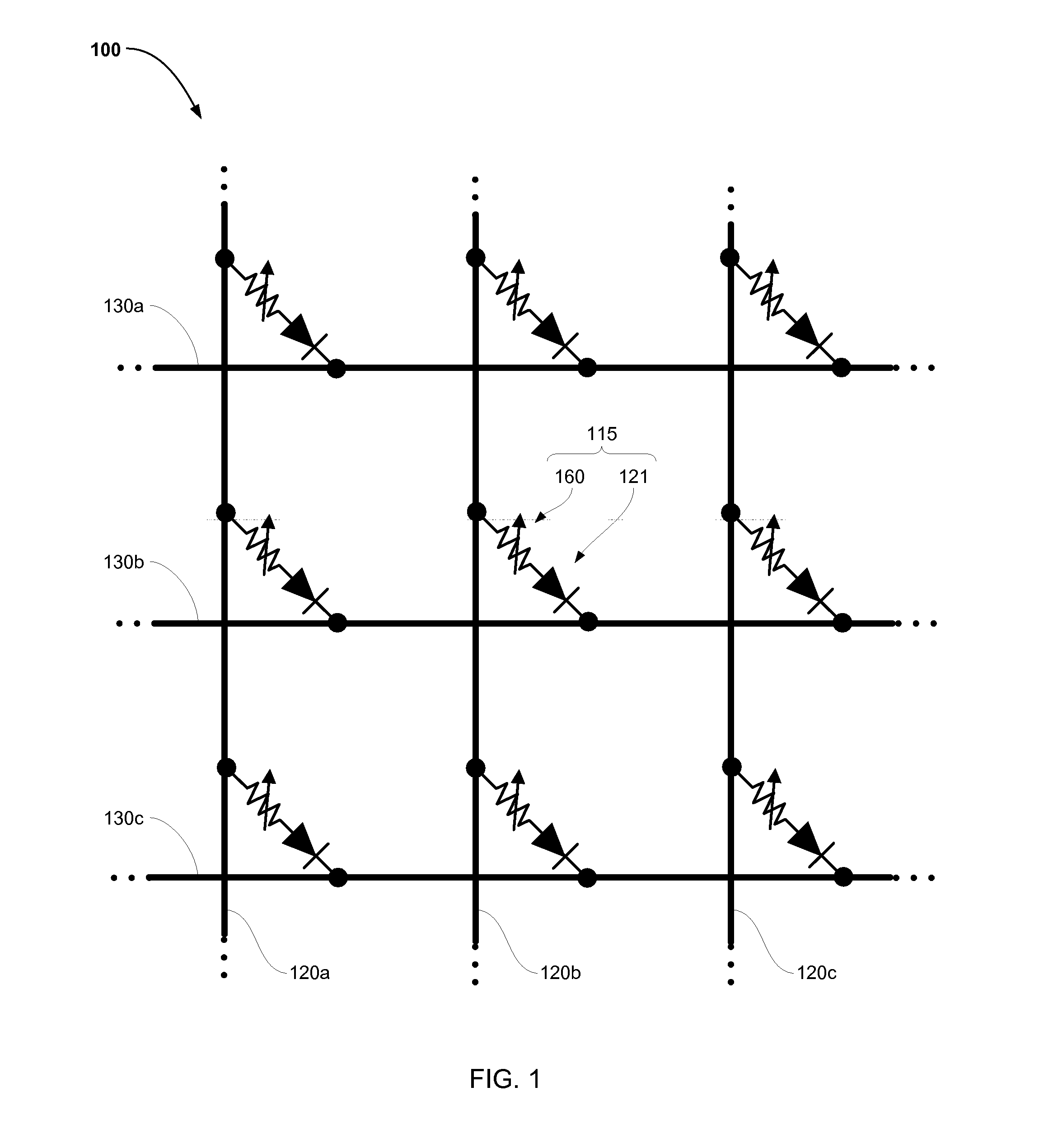
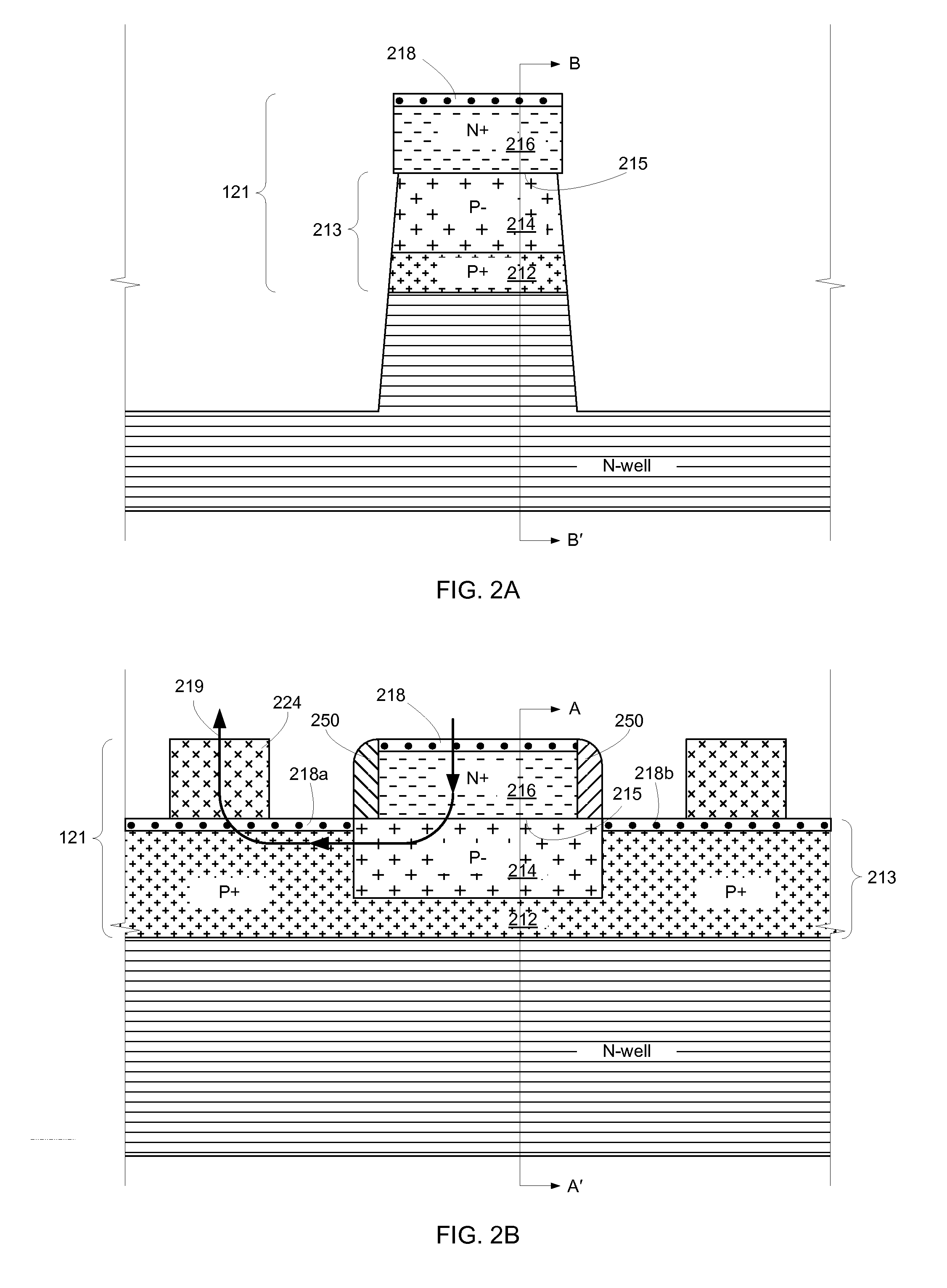
[0056]The invention will now be described in further detail by reference to the drawings, which illustrate alternative specific embodiments and methods. The drawings are diagrammatic, showing features of the embodiments and their relation to other features and structures, and are not made to scale. For improved clarity of presentation, in the figures illustrating various embodiments, elements corresponding to elements shown in other drawings are not all particularly renumbered, although they are all readily identifiable in all the figures. Also for clarity of presentation certain features are not shown in the figures, where not necessary for an understanding of the invention. It is to be understood that there is no intention to limit the invention to the specifically disclosed embodiments and methods but that the invention may be practiced using other features, elements, methods and embodiments. Preferred embodiments are described to illustrate the present invention, not to limit it...


PUM


Abstract

A memory device includes a driver comprising a pn-junction in the form of a multilayer stack including a first doped semiconductor region having a first conductivity type, and a second doped semiconductor region having a second conductivity type opposite the first conductivity type, the first and second doped semiconductors defining a pn-junction therebetween, in which the first doped semiconductor region is formed in a single-crystalline semiconductor, and the second doped semiconductor region includes a polycrystalline semiconductor. Also, a method for making a memory device includes forming a first doped semiconductor region of a first conductivity type in a single-crystal semiconductor, such as on a semiconductor wafer; and forming a second doped polycrystalline semiconductor region of a second conductivity type opposite the first conductivity type, defining a pn-junction between the first and second regions.

Description

CROSS-REFERENCE TO RELATED APPLICATION[0001]The present application is related to U.S. patent application Ser. No. ______, entitled MEMORY CELL ACCESS DEVICE HAVING A PN-JUNCTION WITH POLYCRYSTALLINE PLUG AND SINGLE-CRYSTAL SEMICONDUCTOR REGIONS by the same inventors, filed on the same day as the present application.PARTIES TO A RESEARCH AGREEMENT[0002]International Business Machines Corporation, a New York corporation and Macronix International Corporation, Ltd., a Taiwan corporation, are parties to a Joint Research Agreement.BACKGROUND[0003]1. Field of the Invention[0004]The present invention relates to high density memory devices based on phase change based memory materials, including chalcogenide based materials and other programmable resistive materials, and to methods for manufacturing such devices.[0005]2. Description of Related Art[0006]Phase change based memory materials, such as chalcogenide based materials and similar materials, can be caused to change phase between an am...

Claims


Application Information

Patent Timeline
IPC IPC(8): H01L45/00H01L29/04H01L21/329
CPCG11C13/0004G11C2213/72H01L27/1021H01L27/2409H01L27/2463H01L27/2472H01L29/04H01L29/165H01L29/861H01L29/8616H01L45/04H01L45/06H01L45/085H01L45/1233H01L45/142H01L45/144H01L45/146H01L45/147H01L45/1675H01L45/1683H10B63/20H10B63/82H10B63/80H10N70/245H10N70/20H10N70/8822H10N70/231H10N70/8836H10N70/8828H10N70/8833H10N70/063H10N70/826H10N70/066
Inventor LUNG, HSIANG-LANLAI, ERH-KUNSHIH, YEN-HAOCHEN, YI-CHOUCHEN, SHIH-HUNG
Owner MACRONIX INT CO LTD
Why Eureka
Try Eureka