Organic light emitting diode

A light-emitting diode, organic technology, applied in the manufacturing of electrical components, electric solid-state devices, semiconductor/solid-state devices, etc., can solve the problem of low light extraction efficiency, and achieve the effect of improving light extraction efficiency, improving luminous efficiency, and reducing total reflection phenomenon.

Inactive Publication Date: 2018-03-09
SICHUAN JIUDINGZHIYUAN INTPROP OPERATIONS CO LTD
View PDF0 Cites 0 Cited by
  • Summary
  • Abstract
  • Description
  • Claims
  • Application Information

AI Technical Summary

Problems solved by technology

In this mode, due to the inherent properties of the refractive index, part of the light is refracted in the anode layer after being incident on the anode layer from the light-emitting layer, so that the refraction angle of the anode layer light is greater than the incident angle, because the refraction angle of the anode layer is equal to that of the glass layer The incident angle of the glass layer makes the incident angle of the glass layer larger than the incident angle of the anode layer, even greater than or equal to the critical angle of the glass layer, so that part of the light is totally reflected between the glass layer and the air layer, resulting in low light output efficiency

Method used


Image

  • Organic light emitting diode
  • Organic light emitting diode

Examples


Embodiment Construction

[0014] The following will clearly and completely describe the technical solutions in the embodiments of the present invention with reference to the accompanying drawings in the embodiments of the present invention. Obviously, the described embodiments are only some, not all, embodiments of the present invention. Based on the embodiments of the present invention, all other embodiments obtained by persons of ordinary skill in the art without making creative efforts belong to the protection scope of the present invention.

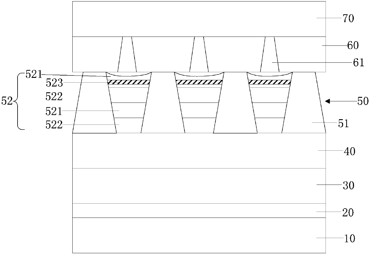
[0015] refer to figure 1 , is a schematic structural diagram of an organic light emitting diode provided by an embodiment of the present invention. The organic light emitting diode of this embodiment includes a silicon carbide substrate 10 , an aluminum nitride buffer layer 20 , a cathode layer 30 , a photosensitive resin layer 40 , an organic layer 50 , an anode layer 60 and a glass panel 70 stacked in sequence.

[0016] The refractive index of the anode lay...


PUM


Abstract

The invention discloses an organic light emitting diode. The organic light emitting diode comprises a silicon carbide substrate, an aluminum nitride buffer layer, a cathode layer, a photosensitive resin layer, an organic layer, an anode layer and a glass panel which are laminated sequentially, wherein the refractive index of the anode layer is higher than that of the glass panel, the organic layercomprises isolation layers distributed on the photosensitive resin layer in a matrix and light emitting layers arranged between the isolation layers, and the surface of each light emitting layer is sunken downwards to form a curved surface; a plurality of through holes are formed in the anode layer and correspond to the light emitting layers in position, each light emitting layer is formed by interleaving and laminating a plurality of gallium nitride layers and a plurality of aluminum gallium nitride layers, a stress buffer layer is inserted into at least one of the plurality of gallium nitride layers, and the lattice constant of the stress buffer layers is larger than that of the gallium nitride layers and the aluminum gallium nitride layers. By means of the organic light emitting diode,the angle range of emergent light can be expanded.

Description

technical field [0001] The invention relates to the technical field of semiconductors, in particular to an organic light emitting diode. Background technique [0002] Most existing organic light-emitting diodes are generally composed of a cathode layer, a light-emitting layer, an anode layer and a glass layer in sequence. Electrons and holes are injected from the cathode and anode respectively, forming excitons in the light-emitting layer and exciting the material of the light-emitting layer to emit light. In this mode, due to the inherent properties of the refractive index, part of the light is refracted in the anode layer after being incident on the anode layer from the light-emitting layer, so that the refraction angle of the anode layer light is greater than the incident angle, because the refraction angle of the anode layer is equal to that of the glass layer The incident angle of the glass layer makes the incident angle of the glass layer larger than the incident angle...

Claims


Application Information

Patent Timeline
Patent Type & Authority Applications(China)
IPC IPC(8): H01L51/50H01L51/52
CPCH10K50/131H10K50/813
Inventor 罗艳
Owner SICHUAN JIUDINGZHIYUAN INTPROP OPERATIONS CO LTD
Why Eureka
Try Eureka