

Display device and manufacturing method thereof
Patent Information
- Authority / Receiving Office
- CN · China
- Patent Type
- Applications(China)
- Current Assignee / Owner
- SAMSUNG DISPLAY CO LTD
- Publication Date
- 2021-06-04
Smart Images
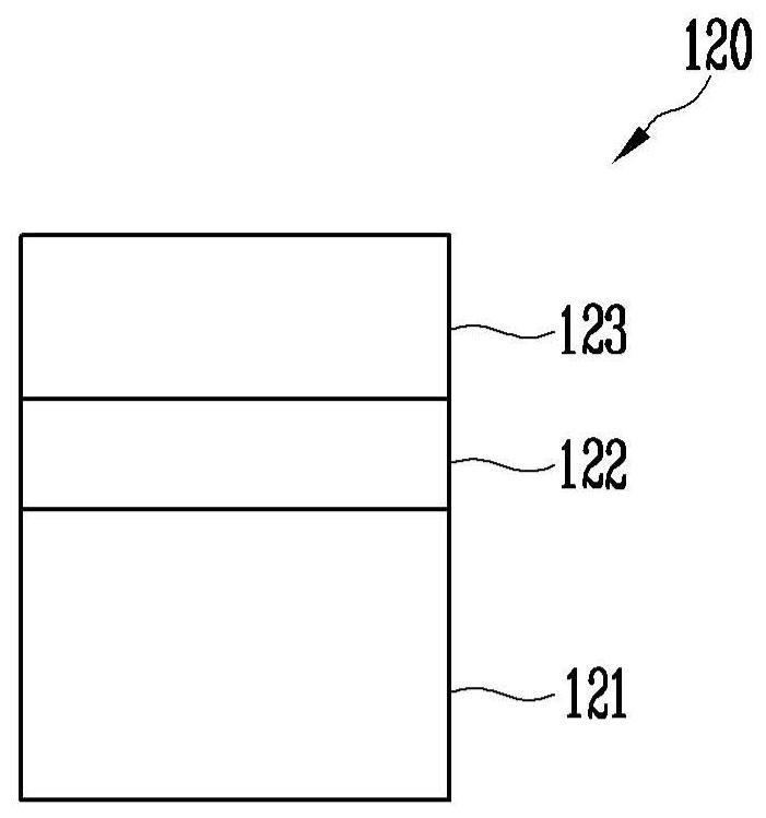
Figure 1 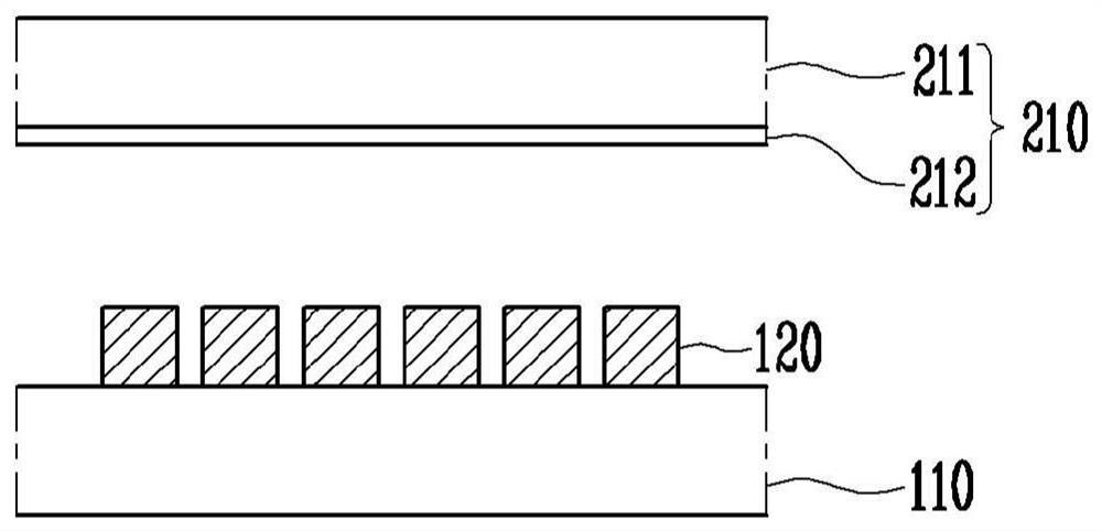
Figure 2 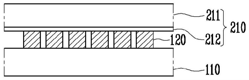
Figure 3
Abstract
Description
technical field
[0001] Various embodiments of the present disclosure relate to a display device and a method of manufacturing the same. Background technique
[0002] A display device displays an image using a combination of light emitted from a plurality of pixels. In a display device, each pixel includes a pixel circuit and a display element controlled in operation by the pixel circuit. A light emitting diode, which is a self-emitting element among display elements, includes a pixel electrode, an emission layer, and a common electrode.
[0003] One of the pixel electrode and the common electrode is an anode for hole injection, and the other is a cathode for electron injection. Holes injected from the anode and electrons injected from the cathode combine in the emission layer to generate excitons, and the excitons release energy to emit light.
[0004] The light emitting diodes may be formed on the backplane by a Pick and Place method or a roll transfer method. However, ...