A metamaterial modulator
A technology of modulators and metamaterials, which is applied in the direction of instruments, antennas, electrical components, etc., can solve the problems of inflexible modulation effects and single modulation performance, and achieve the effects of rich and flexible modulation, high modulation depth, and wide modulation bandwidth
- Summary
- Abstract
- Description
- Claims
- Application Information
AI Technical Summary
Problems solved by technology
Method used
Image
Examples
Embodiment 1
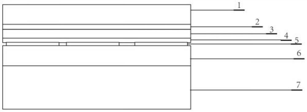
[0056] like figure 1 As shown, an embodiment of the present invention provides a metamaterial modulator, which includes a surface layer 1, a graphene layer 2, a first flexible dielectric layer 3, a perovskite layer 4, a metal structure arranged from top to bottom layer 5, second flexible dielectric layer 6 and underlying substrate layer 7;
[0057] The second flexible dielectric layer 6 is attached to the upper surface of the underlying substrate layer 7 , the metal structure layer 5 is attached to the upper surface of the second flexible dielectric layer 6 , the perovskite layer 4 covers the metal structure layer 5 , and the first flexible dielectric layer 3 It is attached to the upper surface of the perovskite layer 4 , the graphene layer 2 is attached to the upper surface of the first flexible medium layer 3 , and the surface layer 1 is attached to the upper surface of the graphene layer 2 .
[0058] The metal structure layer 5 is composed of several metal structures, and ...
Embodiment 2
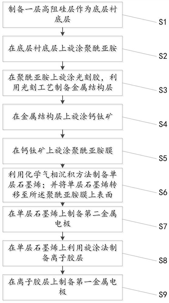
[0078] like Figure 7 As shown, an embodiment of the present invention provides a method for preparing a metamaterial modulator, the method comprising:
[0079] S1, prepare a layer of high-resistance silicon layer as the bottom substrate layer 7 .
[0080] A 500 μm thick high-resistance silicon layer was prepared.
[0081] S2, spin-coating polyimide on the underlying substrate layer 7, the specific steps include:
[0082] Spin coating 10μm thick polyimide film on 500μm high resistance silicon: After cleaning the prepared high resistance silicon, spin coating a polyimide solution with a viscosity of 3600 (centipoise) on the polished surface, and the spin coating time is 60 seconds at 2200RPM. Then, the polyimide solution was baked, and the baking temperature was 120° C., 200° C. and 230° C. for 1 hour each, and then continued to bake at 250° C. for 2 hours.
[0083] S3, spin-coating photoresist on the polyimide, and prepare the metal structure layer 5 by using a photolithogra...
PUM
| Property | Measurement | Unit |
|---|---|---|
| length | aaaaa | aaaaa |
| thickness | aaaaa | aaaaa |
| thickness | aaaaa | aaaaa |
Abstract
Description
Claims
Application Information


