Wafer visual detection method, wafer visual detection system and wafer damage detection method

A visual inspection and wafer technology, applied in semiconductor/solid-state device testing/measurement, electrical components, semiconductor/solid-state device manufacturing, etc., can solve problems such as difficult screening, mixing, wafer inspection, etc., to ensure stability and safety performance, ensure continuous operation, and improve accuracy

Pending Publication Date: 2021-07-23
创微微电子(常州)有限公司 +1
View PDF6 Cites 4 Cited by
  • Summary
  • Abstract
  • Description
  • Claims
  • Application Information

AI Technical Summary

Problems solved by technology

[0002] During the operation of the current wafer cleaning equipment, the wafer box is often placed manually, and the position and angle of the wafer box cannot be monitored during loading.
The position and angle of the wafer box will affect the detection of the number of wafers in the wafer box, and it is not conducive to the transportation of the wafer box, so that there will be damage to the wafer during the cleaning process in the tank. If it is not detected and screened in time, It will cause unqualified products and qualified products to be mixed together, and it is difficult to screen later

Method used


Image

  • Wafer visual detection method, wafer visual detection system and wafer damage detection method
  • Wafer visual detection method, wafer visual detection system and wafer damage detection method
  • Wafer visual detection method, wafer visual detection system and wafer damage detection method

Examples


Embodiment 1

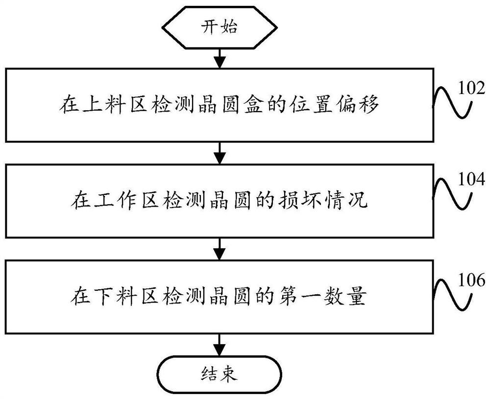
[0039] like figure 1As shown in one embodiment of the present invention, a wafer visual detection method is proposed, including:

[0040] Step 102, in the upper region detecting the positional offset of the wafer cassette;

[0041] Step 104: The damage of the wafer is detected in the work area;

[0042] Step 106: The first number of wafers is detected in the lower material region.

[0043] In this embodiment, the wafer cassette is placed on the transport line at the station by manual or other conveying assembly, and whether the position of the wafer cassette occurs at the stage, that is, the first detecting the deposition of the wafer cassette. A position of the positional offset information of the target placement area of ​​the pre-set upper zone, so that the corresponding position adjustment is made by position offset information such that the first position of the wafer box is placed in the wafer in the wafer. The location is the same. On the one hand, the wafer cassette can be...

Embodiment 2

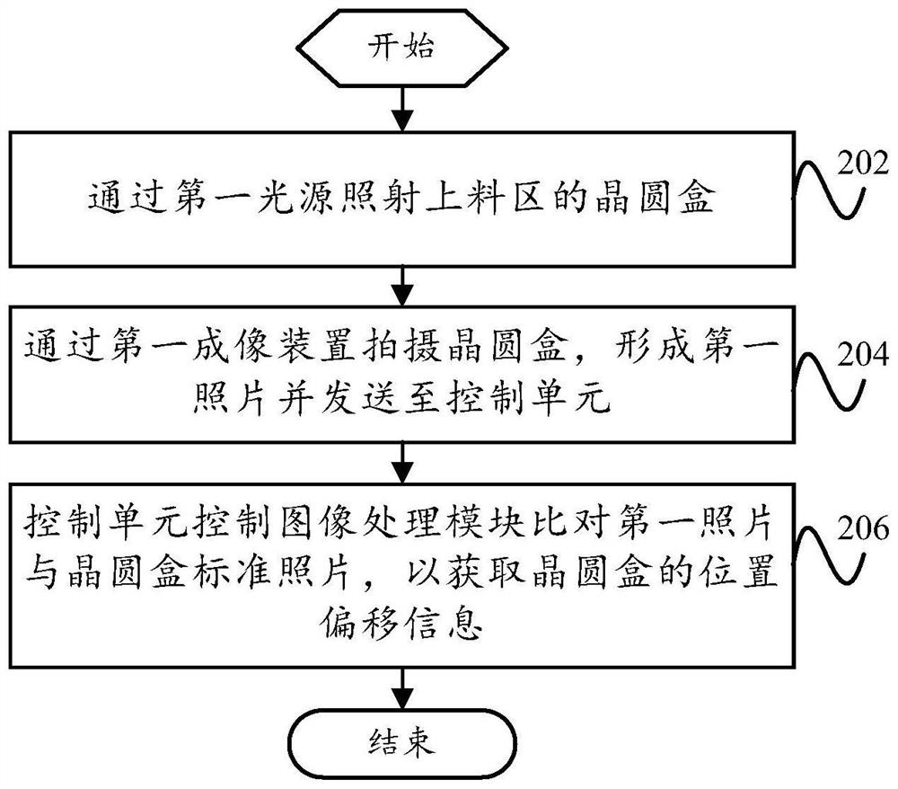
[0049] like figure 2 As shown in one embodiment of the invention, step 102, the positional offset of the wafer cassette in the charge area, including:

[0050] Step 202, through the first light source, the wafer box of the upper material is irradiated;

[0051] Step 204, pass the wafer box by the first imaging device, forming a first photo and transmitted to the control unit;

[0052] Step 206: The control unit controls the image processing module aligned with the first photo and the wafer box standard photos to acquire the positional offset information of the wafer cassette.

[0053] Wherein, the positional offset information of the wafer box includes an offset of the wafer cassette in the plaving angle of the upper region.

[0054] In this embodiment, the wafer cassette of the upper material is irradiated with the wafer visual detection system, to meet the requirements of the shooting light, sharpness of the first imaging device. The wafer cassette is photographed by the first i...

Embodiment 3

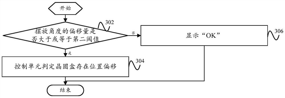
[0060] like image 3 As shown, according to an embodiment of the present invention, the positional offset information of the wafer cassette includes an offset of the wafer cassette in the plaving angle; the wafer visual detection method also includes:

[0061] Step 302, whether the offset of the placed angle is greater than or equal to the second threshold, if yes, enter step 304, if, proceed to step 306;

[0062] Step 304, the control unit determines that the wafer cassette is in position offset;

[0063] Step 306 show "OK".

[0064] In this embodiment, the extension of the wafer cassette in the wafer cassette is obtained by the first photo of the wafer cassette compared to the wafer cassette. The size relationship between the offset of the placement angle and the second threshold is compared. When the offset of the placed angle is greater than or equal to the second threshold, the crystal circular cassette is obvious, and the partial wafer is exceeded at this time. The detection ...


PUM


Abstract

The invention provides a wafer visual detection method, a wafer visual detection system and a wafer damage detection method. The wafer visual detection method comprises the steps of detecting the position offset of a wafer box in a feeding area; detecting the damage condition of the wafer in the working area; and detecting a first number of wafers in a blanking area. Therefore, wafer box positioning, wafer damage condition and wafer number detection in different areas are utilized, a wafer detection mechanism is improved, the accuracy of detection data is guaranteed, a user can monitor the states of the wafers and the wafer boxes in real time, and cost loss caused by equipment abnormity is effectively avoided.

Description

Technical field [0001] The present invention relates to the field of semiconductors, and in particular, a wafer visual detection method, a wafer visual detection system, a method of detecting wafer damage. Background technique [0002] The current wafer cleaning equipment is often placed in manual way, and the position and angle of the wafer cassette cannot be monitored when the wafer is placed. The position and angle of the wafer cassette will affect the detection of the number of wafer in the wafer box, and is not conducive to the transport wafer box such that the wafer is damaged during the cleaning of the slot, and if it is not detected and filtered, It will cause unqualified products to mix together with qualified products, and it is difficult to filter later. Inventive content [0003] The present invention is intended to address at least one of the technical problems present in the prior art or related art. [0004] To this end, the first aspect of the invention provides ...

Claims


Application Information

Patent Timeline
Patent Type & Authority Applications(China)
IPC IPC(8): H01L21/66H01L21/67
CPCH01L22/12H01L22/20H01L21/67288H01L21/67265H01L21/67259H01L21/67253
Inventor 左国军任金枝范生刚马冠男
Owner 创微微电子(常州)有限公司
Why Eureka
Try Eureka