Method for monitoring pollutants in reaction cavity of ion implantation machine

A technology of ion implantation and reaction chamber, which is applied in the direction of measuring devices, instruments, discharge tubes, etc., and can solve problems such as damage to wafers

Inactive Publication Date: 2019-05-21
SHANGHAI HUAHONG GRACE SEMICON MFG CORP
View PDF9 Cites 0 Cited by
  • Summary
  • Abstract
  • Description
  • Claims
  • Application Information

AI Technical Summary

Problems solved by technology

[0004] The purpose of the present invention is to provide a method for monitoring pollutants in the reaction chamber of an ion implantation machine, which is used to monitor the situation of pollutants in the reaction chamber of an ion implantation machine, and solve the problem of damaging the wafer due to the change of the etching rate of polysilicon

Method used


Image

  • Method for monitoring pollutants in reaction cavity of ion implantation machine

Examples


Embodiment Construction

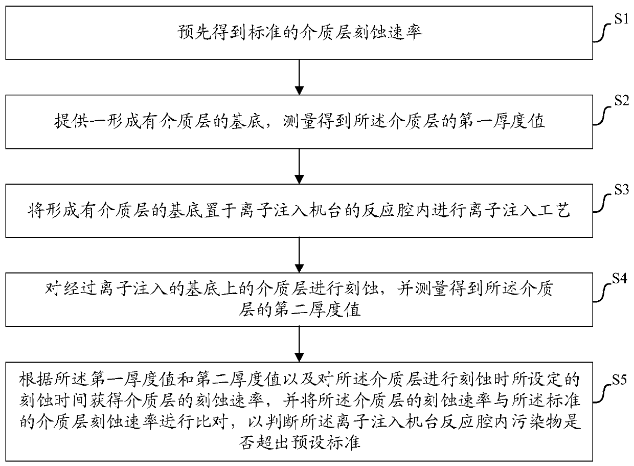
[0019] The invention will be described in more detail below with reference to the accompanying drawings, which show a preferred embodiment of the invention, it being understood that those skilled in the art can modify the invention described herein and still achieve the advantageous effects of the invention. Therefore, the following description should be understood as the broad knowledge of those skilled in the art, but not as a limitation of the present invention.

[0020] In the interest of clarity, not all features of an actual embodiment are described. In the following description, well-known functions and constructions are not described in detail since they would obscure the invention with unnecessary detail. It should be appreciated that in the development of any actual embodiment, numerous implementation details must be worked out to achieve the developer's specific goals, such as changing from one embodiment to another in accordance with system-related or business-rela...


PUM


Abstract

The invention discloses a monitoring method for pollutants in a reaction cavity of an ion implantation machine. The monitoring method comprises the following steps: obtaining a standard dielectric layer etching rate in advance; providing a substrate with a dielectric layer, and measuring to obtain a first thickness value of the dielectric layer; placing the substrate on which the dielectric layeris formed in the reaction cavity of the ion implantation machine for ion implantation; etching the dielectric layer on the substrate after ion implantation, and measuring the dielectric layer to obtain a second thickness value of the dielectric layer; and obtaining the etching rate of the dielectric layer according to the first thickness value, the second thickness value and the set etching time when the dielectric layer is etched, and comparing the etching rate of the dielectric layer with the standard etching rate of the dielectric layer. The problem that a wafer is damaged due to the changeof the etching rate of the product can be solved.

Description

technical field [0001] The invention relates to the technical field of integrated circuit manufacturing, in particular to a method for monitoring pollutants in a reaction chamber of an ion implantation machine. Background technique [0002] During the long-term use of the ion implantation machine, many pollutants will be formed in the reaction chamber, and these pollutants are often formed with many uncertainties. Some of the pollutants will interact with the wafers in the reaction chamber. The reaction of polysilicon changes the chemical properties of polysilicon, resulting in subsequent etching of polysilicon, and its etching rate will change, causing irreversible damage to the product. For example, due to changes in the chemical properties of polysilicon, the etching rate becomes faster when the polysilicon is subsequently etched, so that under the same etching conditions, the polysilicon is over etched, and the oxide layer under the polysilicon is over etched. Etching o...

Claims


Application Information

Patent Timeline
Patent Type & Authority Applications(China)
IPC IPC(8): G01B21/08H01J37/317H01L21/67
Inventor 范世炜
Owner SHANGHAI HUAHONG GRACE SEMICON MFG CORP
Why Eureka
Try Eureka