A full gan integrated gate drive circuit with dead time control

A dead-time control and drive circuit technology, applied in electrical components, high-efficiency power electronic conversion, output power conversion devices, etc., to achieve the effect of reducing static leakage

Active Publication Date: 2022-05-24
UNIV OF ELECTRONICS SCI & TECH OF CHINA
View PDF6 Cites 0 Cited by
  • Summary
  • Abstract
  • Description
  • Claims
  • Application Information

AI Technical Summary

Problems solved by technology

In practical applications, due to the unique device characteristics of GaN, the drive of Si-based MOS power devices cannot be simply used as the drive of GaN power devices, and the drive circuit of GaN power devices needs to be designed separately

Method used


Image

  • A full gan integrated gate drive circuit with dead time control
  • A full gan integrated gate drive circuit with dead time control
  • A full gan integrated gate drive circuit with dead time control

Examples


Embodiment approach

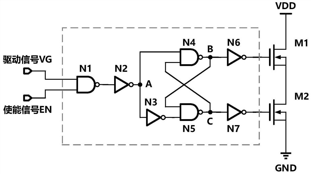
[0020] The present invention proposes a full GaN integrated gate drive circuit with dead time control, such as Figure 1 Shown, comprising 3 and non-gate circuits N1, N4 and N5, 4 non-gate circuits N2, N3, N6 and N7.

[0021] The specific circuit structure has been elaborated in the content portion of the invention, which will not be repeated here.

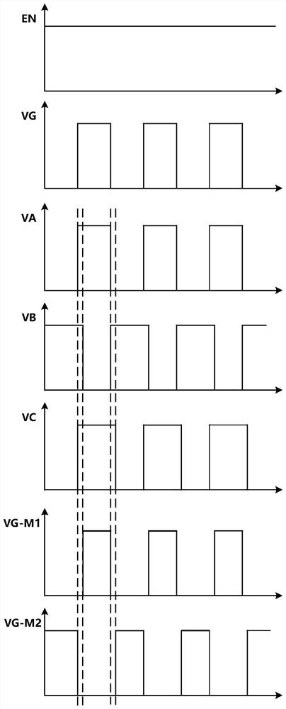
[0022] The following embodiment of the present invention in conjunction with the accompanying drawings to provide a half-bridge circuit pass-through protection circuit working principle and process in detail:

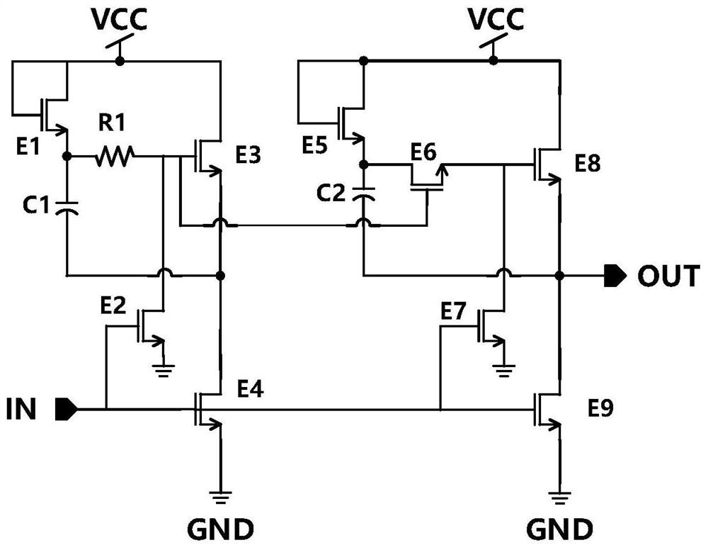
[0023] as Figure 3As shown, the non-gate circuit contains nine transistors E1, E2, E3, E4, E5, E6, E7, E8, and E9, two capacitors C1 and C2, and one resistor R1. Among them, E1, E2, E3, E4, C1 and R1 constitute the secondary side of the non-gate circuit, and E5, E6, E7, E8, E9 and C2 constitute the main side of the non-gate circuit. Transistor E7 in the main stage side plays the role of pull-down the gate potential of transistor...


PUM


Abstract

The invention discloses an all-GaN integrated gate drive circuit with dead time control, which realizes the basic digital logic gate circuit of all-GaN integration through the enhanced GaN transistor, that is, the low-power NOT gate circuit and the NAND gate circuit, further Using these basic digital logic gates and introducing a feedback structure, an all-GaN integrated gate driver circuit with dead time control is realized. The circuit effectively avoids the punch-through phenomenon caused by the high-side power device and the low-side power device being turned on at the same time in the half-bridge structure. Leakage, laying the foundation for the full GaN integration of the driver stage and power stage in the power conversion circuit in the future.

Description

Technical field [0001] The present invention belongs to the field of GaN power electronics, specifically relates to a full GaN integrated gate drive circuit with dead time control. Background [0002] In recent years, devices based on Gallium Nitride (GaN) materials have developed rapidly, and as a new generation of semiconductor materials that have emerged in the past 20 years, they have many performance advantages. Compared with Si materials, the physical properties of GaN materials have the advantages of wide band gap width, high melting point (high temperature resistance, radiation resistance), high breakdown field strength and high pressure resistance, fast electron saturation drift speed (high frequency operation), and high thermal conductivity, making GaN devices more suitable for working in high temperature, high pressure and high frequency applications. GaN as a third-generation semiconductor material is widely used in the field of power electronics technology, in the po...

Claims


Application Information

Patent Timeline
Patent Type & Authority Patents(China)
IPC IPC(8): H02M1/08H02M1/088H02M1/38
CPCH02M1/08H02M1/088H02M1/38Y02B70/10
Inventor 周琦韩晓琦党其亮罗志华邓超
Owner UNIV OF ELECTRONICS SCI & TECH OF CHINA
Why Eureka
Try Eureka