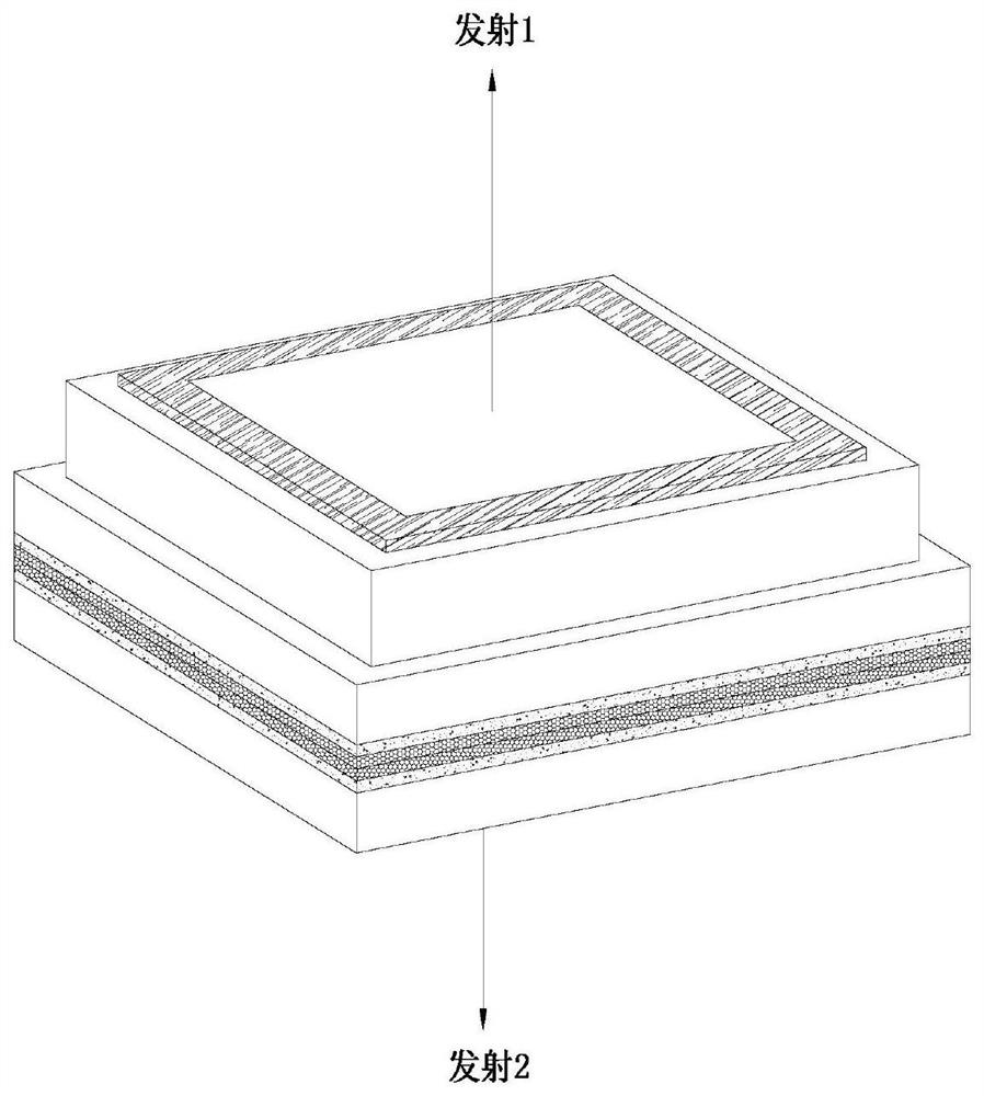
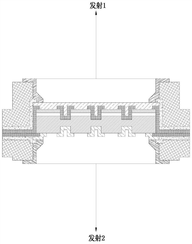
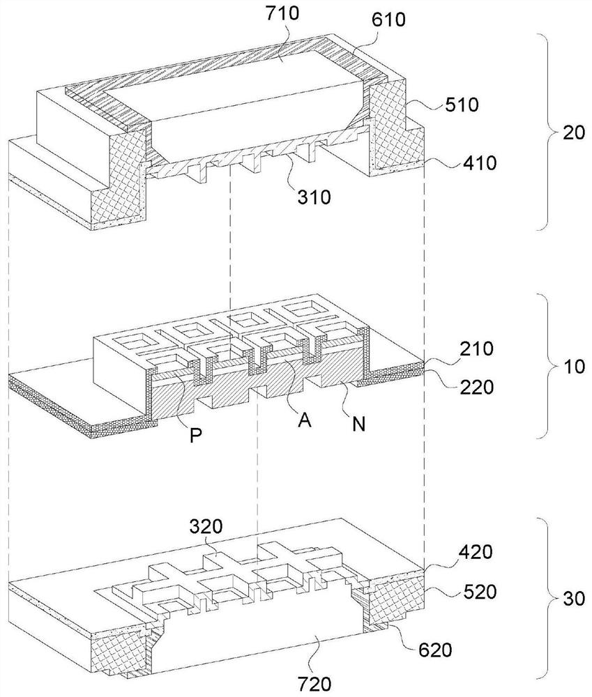
Dual emission LED chip
An LED chip, double-sided light-emitting technology, applied in electrical components, circuits, semiconductor devices, etc., can solve the problems of power consumption, manufacturing cost, thickening of thickness, etc., to achieve miniaturization, reduce total internal reflection, and reduce manufacturing costs. Effect
- Summary
- Abstract
- Description
- Claims
- Application Information
AI Technical Summary
Problems solved by technology
Method used
Image

Examples
no. 1 example
[0073] On the other hand, in the P-N junction 10, heat is generated together with the light emitting effect. Therefore, the P-N junction 10 may have a mesa structure, which promotes heat generation by increasing the surface area of each layer. Here, the "mesa structure" refers to a structure in which a plurality of islands are formed by engraving the surface of each layer to a predetermined depth, and the edge of each island is a vertical cliff or slope. According to the first embodiment of the present invention, the P-N junction includes a P-direction mesa structure PMS formed on the surface of the P layer and an N-direction mesa structure NMS formed on the surface of the N layer.
[0074] The P-direction mesa structure PMS is a mesa structure formed by engraving from the upper surface of the P layer P to a predetermined depth of the N layer N, forming a plurality of P-direction islands 110 . The number of P-direction islands 110 may vary according to design. Since the P-...
PUM
 Abstract
Description
Claims
Application Information
 - R&D Engineer
- R&D Manager
- IP Professional
- Industry Leading Data Capabilities
- Powerful AI technology
- Patent DNA Extraction
Browse by: Latest US Patents, China's latest patents, Technical Efficacy Thesaurus, Application Domain, Technology Topic.
© 2024 PatSnap. All rights reserved.Legal|Privacy policy|Modern Slavery Act Transparency Statement|Sitemap