Adsorption type chip transfer device and chip repair device

A chip transfer and adsorption technology, used in electric heating devices, auxiliary devices, welding equipment, etc., can solve problems such as chip damage, and achieve the effect of facilitating installation operations, improving loading efficiency and loading quality, and avoiding collapse and deformation.

Pending Publication Date: 2021-09-07
QUICK INTELLIGENT EQUIP CO LTD
View PDF0 Cites 5 Cited by
  • Summary
  • Abstract
  • Description
  • Claims
  • Application Information

AI Technical Summary

Problems solved by technology

When mounting chips, the suction nozzle moves down and contacts the chip, and then the chip is sucked by the suction nozzle and transferred to the position to be soldered on the circuit board. During this process, if the downward stroke of the suction nozzle is not properly controlled, the suction nozzle will Applying a large pressure to the chip may easily cause the chip to be damaged due to excessive pressure

Method used


Image

  • Adsorption type chip transfer device and chip repair device
  • Adsorption type chip transfer device and chip repair device
  • Adsorption type chip transfer device and chip repair device

Examples


Embodiment 1

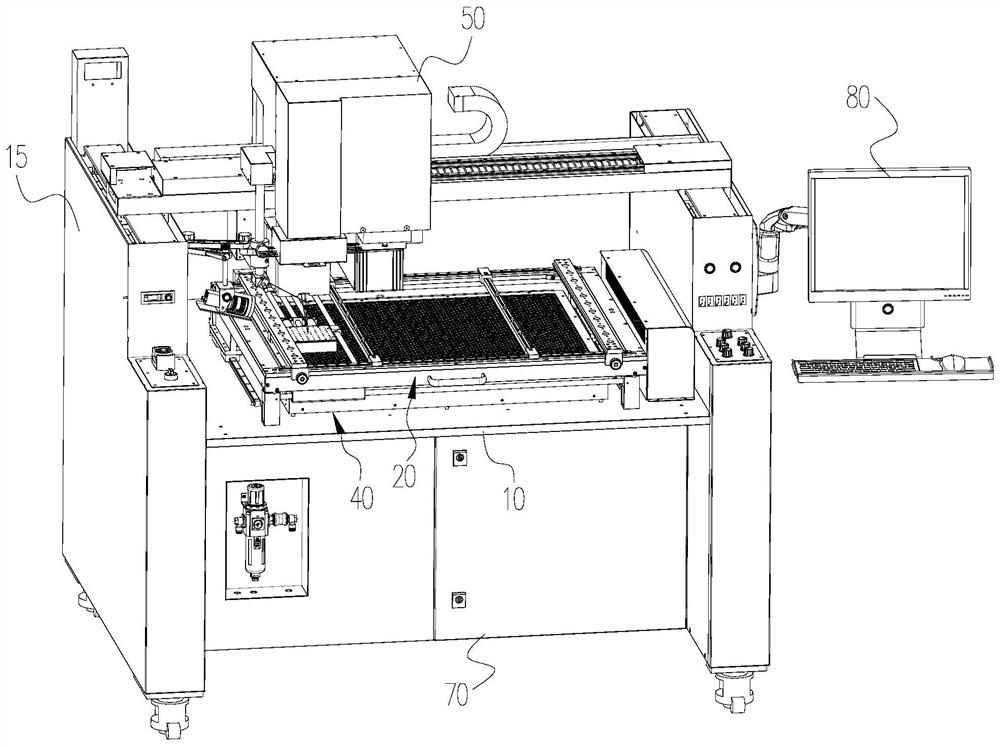
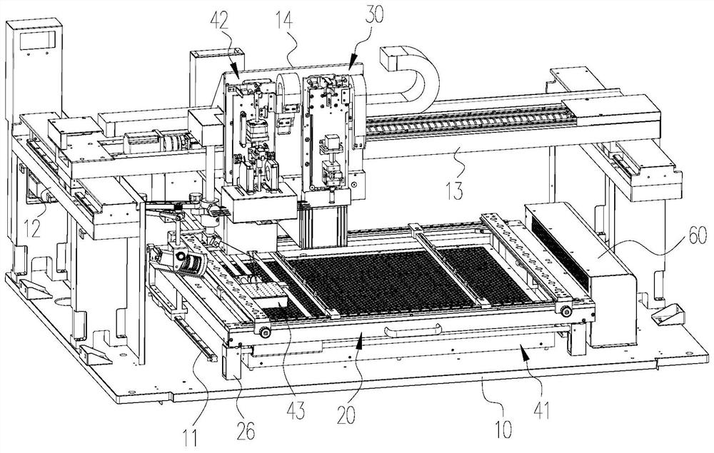
[0093] see figure 1 , figure 2 , the present invention provides a chip rework equipment for desoldering, transfer and soldering of chips, the chip rework equipment includes a machine platform 10, a stage mechanism 20 arranged on the machine platform 10 and used for placing chips, which can The adsorption type chip transfer device 30 that is movably arranged on the stage mechanism 20 and the heating device 40 installed on the machine platform 10, wherein the stage mechanism 20 is used to load a fixed circuit board, and the adsorption type chip transfer device 30 is used to transfer The chip is transferred to the mounting position of the circuit board, and the heating device 40 is used to heat the circuit board to facilitate desoldering and welding.

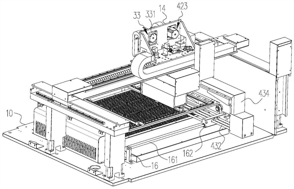
[0094] see Figure 4 The stage mechanism 20 includes a sliding seat 21 slidably arranged on the machine table 10, a frame 22 reversibly installed on the sliding seat 21, and a support plate 23 and a support rod slidably arranged...

Embodiment 2

[0141] see Figure 18 Embodiment 2 of the present invention provides a chip rework device. The difference between the chip rework device and Embodiment 1 is that the structure of the desoldering heating mechanism 42 of the present invention is different, specifically the structure of the heating module 424 is different.

[0142] Specifically, the heating module 424 in the second embodiment includes a hot air mixing chamber 4248 installed on the sliding plate 422, a cartridge heater 4249 installed on the top of the hot air mixing chamber 4248, and a hot air nozzle installed at the bottom of the hot air mixing chamber 4248. 4250, the cartridge heater 4249 is connected to the blower through the air pipe joint 4251. When in use, the wind generated after the fan is started is heated by the cartridge heater 4249 and enters the hot air mixing chamber 4248, and then passes through the hot air nozzle 4250 Flow to the part of the chip to be desoldered.

[0143] In addition, in order to...


PUM


Abstract

The invention discloses an adsorption type chip transfer device which comprises a base plate, a sliding plate, a driving assembly, a movable seat, a suction rod, a suction nozzle and an elastic piece. The sliding plate is arranged on the base plate in a sliding manner along the longitudinal direction, the driving assembly drives the sliding plate to move, and the movable seat is arranged on the sliding plate in a sliding manner along the longitudinal direction; the suction rod is installed on the movable seat and is connected with a vacuum generator, the suction nozzle is connected to the lower end of the suction rod, the elastic part is telescopically arranged between the sliding plate and the movable seat along the sliding direction of the movable seat, and the movable seat abuts against the upper end of the elastic part, so that the movable seat is suspended on the sliding plate. According to the adsorption type chip transfer device, the chip is buffered when the chip is adsorbed, the situation that the chip is damaged due to excessive pressure in the chip adsorption process is effectively overcome, and the lossless transfer of the chip is achieved. The invention further discloses a chip repair device with the adsorption type chip transfer device.

Description

technical field [0001] The invention relates to the technical field of chip transfer, in particular to an adsorption-type chip transfer device and chip rework equipment. Background technique [0002] In the process of GBA chip rework, chip rework equipment is usually used for operation, which is mainly responsible for desoldering, mounting and welding of chips. When mounting chips, the suction nozzle moves downward and contacts the chip, and then the chip is sucked by the suction nozzle and transferred to the position to be soldered on the circuit board. During this process, if the downward stroke of the suction nozzle is not properly controlled, the suction nozzle will Applying a large pressure to the chip may easily cause the chip to be damaged due to excessive pressure. [0003] Therefore, in the field of chip rework technology, how to realize the lossless transfer of chips has become an urgent problem to be solved in this field. Contents of the invention [0004] Bas...

Claims


Application Information

Patent Timeline
Patent Type & Authority Applications(China)
IPC IPC(8): H01L21/677H01L21/683B23K1/018B23K3/04B23K3/08
CPCH01L21/6838H01L21/67742B23K1/018B23K3/04B23K3/08B23K2101/36
Inventor 陈魏潘兵
Owner QUICK INTELLIGENT EQUIP CO LTD
Why Eureka
Try Eureka