Circuit board assembly, circuit board stacking structure and electronic equipment

A technology of circuit board assembly and stacking structure, which is applied to the structural connection of printed circuits, printed circuit components, printed circuits, etc., can solve the problems that the integration degree and utilization rate of circuit boards cannot be further improved.

Active Publication Date: 2021-11-19
VIVO MOBILE COMM CO LTD
View PDF6 Cites 1 Cited by
  • Summary
  • Abstract
  • Description
  • Claims
  • Application Information

AI Technical Summary

Problems solved by technology

[0004] The invention proposes a circuit board assembly, a circuit board stacking structure and electronic equipment to solve the problem that the integration degree and utilization rate of the circuit board cannot be further improved

Method used


Image

  • Circuit board assembly, circuit board stacking structure and electronic equipment
  • Circuit board assembly, circuit board stacking structure and electronic equipment
  • Circuit board assembly, circuit board stacking structure and electronic equipment

Examples


Embodiment Construction

[0045] In order to make the purpose, technical solution and advantages of the present application clearer, the technical solution of the present application will be clearly and completely described below in conjunction with specific embodiments of the present application and corresponding drawings. Apparently, the described embodiments are only some of the embodiments of the present application, rather than all the embodiments. Based on the embodiments in this application, all other embodiments obtained by persons of ordinary skill in the art without making creative efforts belong to the scope of protection of this application.

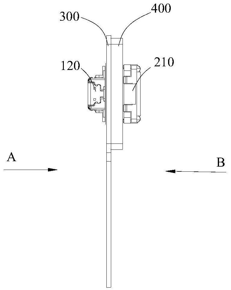
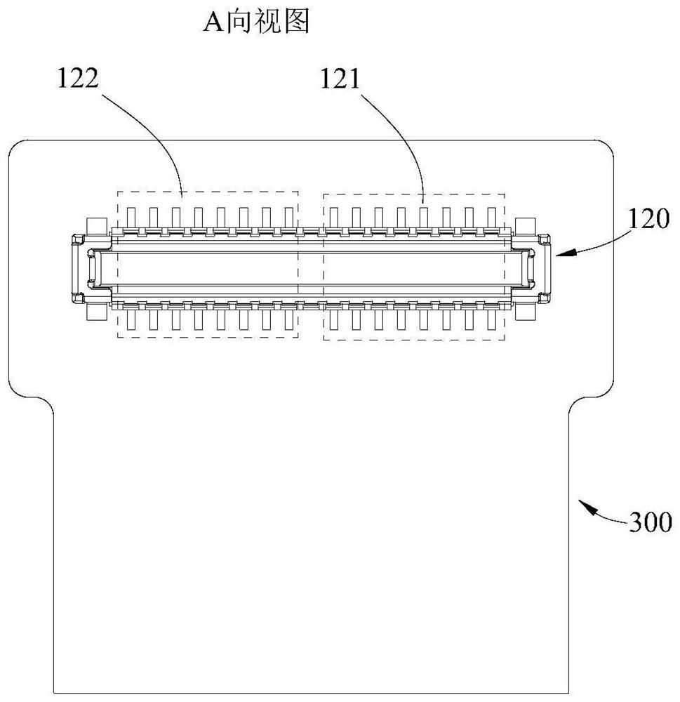
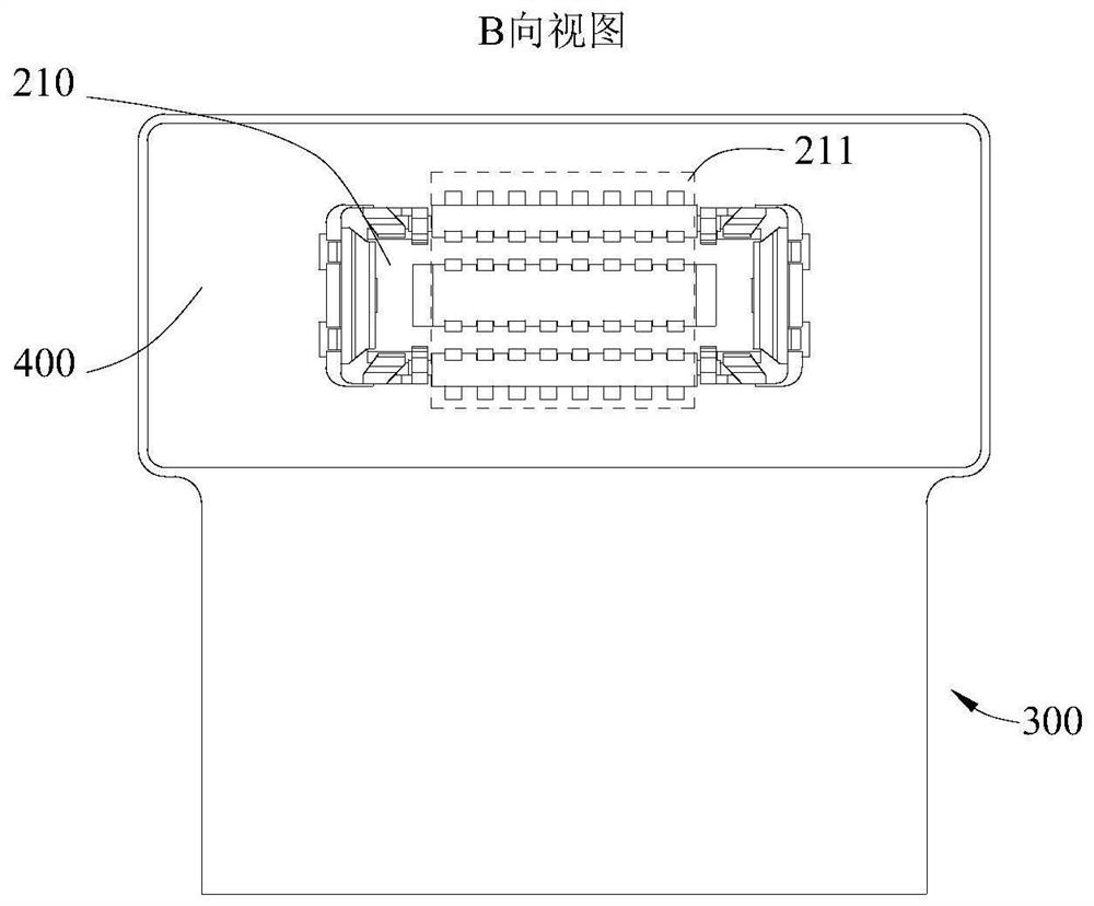
[0046] like Figure 1 to Figure 13 As shown, the present application discloses a circuit board stacking structure, which may include a third circuit board 700 , a circuit board assembly and a second circuit board 500 stacked in sequence.

[0047] The third circuit board 700 may be a main board, which serves as the installation base of the circuit boa...


PUM


Abstract

The invention discloses a circuit board stacking structure which comprises a third circuit board, a circuit board assembly and a second circuit board sequentially stacked. The circuit board assembly comprises a first connector, a first circuit board and a second connecting seat which are sequentially stacked, the first connector is provided with a second electric connection part and a second connecting part, and the second connecting seat is provided with a fourth connecting part. The first circuit board is provided with a third electric connection part and a third connection part, the first circuit board is provided with a fourth electric connection part, and a first wire, the third connection part and the second connection part in the first circuit board are electrically connected in sequence, so that a second path is formed between the first circuit board and the third circuit board; and the fourth connection part, the fourth electric connection part, the third electric connection part and the second electric connection part are electrically connected in sequence, so that a first path is formed between the second circuit board and the third circuit board, according to the circuit board stacking structure, more circuit boards can be arranged while the wiring area is not changed, the integration level and the utilization rate are improved, and the power supply requirements of more functional devices are met.

Description

technical field [0001] The present application relates to the technical field of electronic equipment, in particular to a circuit board assembly, a circuit board stacking structure and electronic equipment. Background technique [0002] With the continuous development of electronic equipment, internal components are also increasing. Taking mobile phones as an example, various functional components in mobile phones, such as lenses, memory, graphics cards, etc., need to be connected to circuit boards to achieve power supply. [0003] In related technologies, circuit boards are usually laid in parallel on the main board to realize their own power supply. However, in such an arrangement, the number of circuit boards that can be arranged is limited when the layout area on the main board is limited. The number of functional devices that can be installed will be limited, and the integration and utilization of the circuit board cannot be further improved. Contents of the invention...

Claims


Application Information

Patent Timeline
Patent Type & Authority Applications(China)
IPC IPC(8): H05K1/18H05K1/14
CPCH05K1/184H05K1/144
Inventor 林协源
Owner VIVO MOBILE COMM CO LTD
Why Eureka
Try Eureka