Lossless Synchronous Absorption Circuit, Boost and Buck Switching Power Supply Circuit

A technology of absorbing circuit and absorbing capacitor, applied in electrical components, adjusting electric variables, instruments, etc., can solve problems such as common mode interference

Pending Publication Date: 2019-01-08
宁波市北仑临宇电子科技有限公司
View PDF0 Cites 1 Cited by
  • Summary
  • Abstract
  • Description
  • Claims
  • Application Information

AI Technical Summary

Problems solved by technology

Since d(VD1)≠0 during the switching process of the switching device Q1, then i1≠0, i1+i2=i1≠0, so the sw

Method used


Image

  • Lossless Synchronous Absorption Circuit, Boost and Buck Switching Power Supply Circuit
  • Lossless Synchronous Absorption Circuit, Boost and Buck Switching Power Supply Circuit
  • Lossless Synchronous Absorption Circuit, Boost and Buck Switching Power Supply Circuit

Examples


Embodiment 1

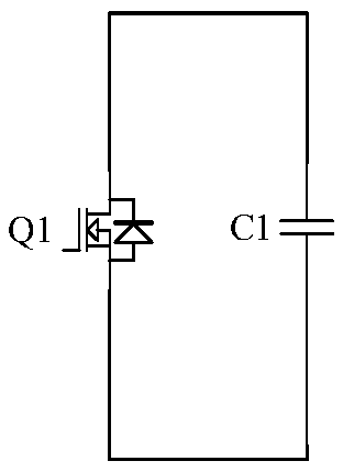
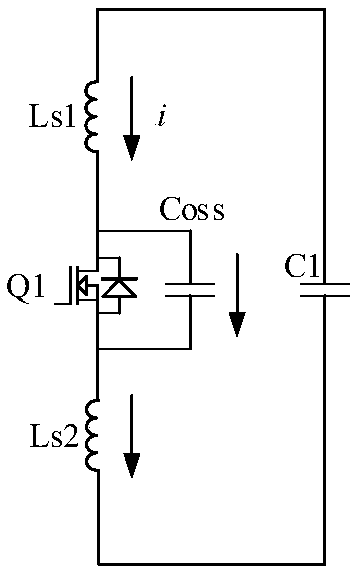
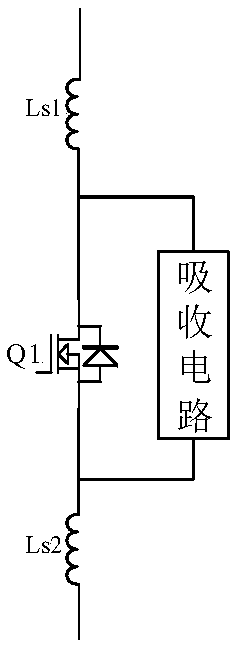
[0048] Please refer to Figure 11 , Embodiment 1 of the present invention provides a lossless synchronous snubber circuit, comprising a first diode Ds1 connected in series with a switching device Q1, a bus capacitor Cbus and a second diode Ds2, the cathode of the first diode Ds1 and A snubber capacitor Cs1 is connected between the common intersection of the bus capacitor Cbus and the common intersection of the anode of the second diode Ds2 and the bus capacitor Cbus, and the switching device is turned on or off by a pulse drive signal. That is, a loss synchronous snubber circuit composed of the first diode Ds1, the bus capacitor Cbus, the second diode Ds2 and the snubber capacitor Cs1 is connected to both ends of the switching device Q1.

[0049] Please refer to Figure 11 , the switching device Q1 may be a field effect transistor. The specific connection relationship is as follows: the drain of the switching device Q1 is connected to the anode of the first diode Ds1, the fi...

Embodiment 2

[0065] Embodiment 2 of the present invention is improved on the basis of Embodiment 1, and its area is that at least one of the first diode Ds1 and the second diode Ds2 in the charging circuit adopts a junction field effect Transistor, bipolar transistor, insulated gate bipolar transistor, metal oxide semiconductor field effect transistor or V-groove field effect transistor replacement, when replacing at least one diode in the charging circuit, said junction field effect transistor, bipolar The conduction direction of the polar transistor, the insulated gate bipolar transistor, the metal oxide semiconductor field effect transistor or the V-groove field effect transistor is the same as the current direction of the charging circuit.

[0066] Wherein, the insulated gate bipolar transistor or the metal oxide semiconductor field effect transistor may be integrated with a diode. When at least one diode in the charging circuit is replaced by an insulated gate bipolar transistor or a ...


PUM


Abstract

A lossless synchronous absorption circuit a step-up and step-down switching power supply circuit, the lossless synchronous absorbing circuit comprising a charging loop composed of a first diode, an absorbing capacitor and a second diode when the switching device is turned off, for causing the absorbing capacitor to absorb the spike voltage energy generated by the switching device through the firstdiode and the second diode; A discharge circuit composed of an absorbing capacitor and a bus capacitor is used for discharging the bus capacitor when the voltage absorbed by the absorbing capacitor is higher than the voltage of the bus capacitor, so that the voltage energy of the absorbing capacitor is fed back to the bus capacitor to realize the lossless absorption of the voltage energy. The invention can effectively suppress the peak voltage of the switching device when the switching device is turned off, and realize lossless absorption and common-mode interference suppression.

Description

technical field [0001] The invention relates to the technical field of switching power supplies, in particular to a lossless synchronous absorbing circuit, a step-up switching power supply circuit and a step-down switching power supply circuit. Background technique [0002] In the field of switching power supply technology, the main components of the switching power supply are switching devices. Since the switching device needs to be connected to other components through wires in the power circuit, and the wires and even the pins of the switching device have parasitic inductance, the switch Both the length and width of the wire in the connection loop of the device affect the size of the parasitic inductance, and the way the wire is laid out in the printed circuit board affects the size of the parasitic inductance. figure 1 It is a simple schematic diagram of the output circuit of the switching device. Please refer to figure 1 , the switching device Q1 forms a current loop ...

Claims


Application Information

Patent Timeline
IPC IPC(8): H02M1/34H02M3/155
CPCH02M1/34H02M3/155H02M1/348
Inventor 袁媛李跃松张迪李佳航
Owner 宁波市北仑临宇电子科技有限公司
Why Eureka
Try Eureka