Array substrate, handwriting board and manufacturing method

A technology for array substrates and manufacturing methods, applied in optics, instruments, electrical digital data processing, etc., can solve problems such as cumbersome manufacturing processes, achieve wide application prospects, simplify manufacturing processes and costs, and solve the effects of cumbersome manufacturing processes

Pending Publication Date: 2021-12-24
HEFEI XINSHENG OPTOELECTRONICS TECH CO LTD +1
View PDF0 Cites 0 Cited by
  • Summary
  • Abstract
  • Description
  • Claims
  • Application Information

AI Technical Summary

Problems solved by technology

However, the production process of most handwriting boards is cumbersome at present.

Method used


Image

  • Array substrate, handwriting board and manufacturing method
  • Array substrate, handwriting board and manufacturing method
  • Array substrate, handwriting board and manufacturing method

Examples


Embodiment Construction

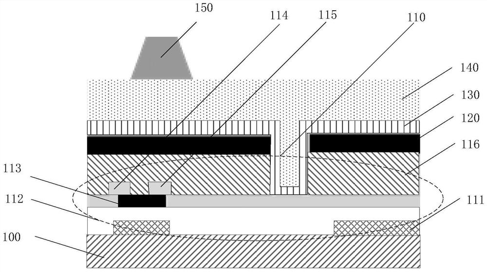
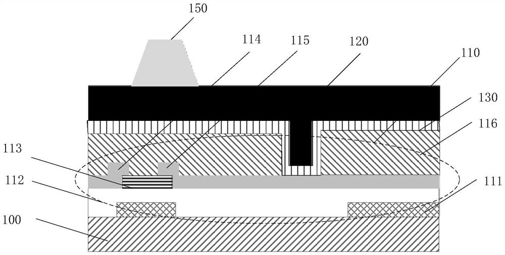
[0045] In order to illustrate the present invention more clearly, the present invention will be further described below in conjunction with preferred embodiments and accompanying drawings. Similar parts in the figures are denoted by the same reference numerals. Those skilled in the art should understand that the content specifically described below is illustrative rather than restrictive, and should not limit the protection scope of the present invention.

[0046] It should be noted that "on", "formed on" and "arranged on" mentioned in this article may mean that one layer is directly formed or set on another layer, or that a A layer is indirectly formed or disposed on another layer, ie there are other layers between the two layers. In this document, unless otherwise specified, the term "on the same layer" used means that two layers, parts, members, elements or parts can be formed by the same patterning process, and that the two layers, parts, members, Elements or parts are g...


PUM


Abstract

The invention discloses an array substrate applied to a handwriting board, the handwriting board and a manufacturing method. The array substrate in one embodiment comprises a drive circuit layer arranged on a first substrate and a colored film layer arranged on the drive circuit layer. According to the array substrate, the colored film layer is arranged on the drive circuit layer, the manufacturing process is effectively simplified, the cost is effectively reduced, the problem that in the prior art, due to the fact that the colored film layer is arranged on the side, away from the drive circuit layer, of the substrate, the manufacturing process is tedious is solved, and the array substrate has wide application prospects.

Description

technical field [0001] The invention relates to the field of display technology, in particular to an array substrate, a tablet and a manufacturing method. Background technique [0002] In the past two years, paperless office has become the new darling of technology applications. Handwriting tablets with writing and display functions are expected to replace some traditional writing tools such as blackboards and whiteboards in education and office fields. The handwriting board only needs something similar to a pen to write, and does not consume auxiliary materials. For the field of education, it can protect the health of teachers and students. However, the production process of most handwriting boards is relatively cumbersome at present. Contents of the invention [0003] In order to solve at least one of the above problems, the first embodiment of the present invention provides an array substrate, which is applied to a tablet, including: a driving circuit layer disposed on...

Claims


Application Information

Patent Timeline
IPC IPC(8): G06F3/044G06F3/041G02F1/1362G02F1/1333
CPCG06F3/0445G06F3/04164G02F1/1362G02F1/13338G06F2203/04103
Inventor 李井森詹成勇马健胡金良
Owner HEFEI XINSHENG OPTOELECTRONICS TECH CO LTD
Why Eureka
Try Eureka