
Pixel charging method and display panel

A pixel charging and display panel technology, applied to static indicators, instruments, etc., can solve problems such as power interference, poor crosstalk in the display horizontal direction, and power supply voltage offset, and achieve high charging rate and avoid bad crosstalk in the horizontal direction.

Pending Publication Date: 2022-01-28
TCL CHINA STAR OPTOELECTRONICS TECH CO LTD
View PDF4 Cites 1 Cited by
  • Summary
  • Abstract
  • Description
  • Claims
  • Application Information

AI Technical Summary

Problems solved by technology

[0004] This application provides a pixel charging method and a display panel to solve the problem that the power supply voltage will shift with the polarity direction when there is a time difference between the output of the positive polarity signal and the negative polarity signal while ensuring a high overall charging rate , and power supply interference occurs, the power supply interference will have an impact on the common electrode voltage, resulting in the technical problem of poor crosstalk in the horizontal direction during display

Method used


Image

  • Pixel charging method and display panel
  • Pixel charging method and display panel
  • Pixel charging method and display panel

Examples


Embodiment Construction

[0044] The technical solutions in the embodiments of the present application will be clearly and completely described below in conjunction with the drawings in the embodiments of the present application. Apparently, the described embodiments are only some of the embodiments of the present application, rather than all the embodiments. Based on the embodiments in this application, all other embodiments obtained by those skilled in the art without making creative efforts belong to the scope of protection of this application. It should be understood that the specific implementations described here are only used to illustrate and explain the present application, and are not intended to limit the present application. The terms "first", "second" and the like in the claims of the present application and the description are used to distinguish different objects, rather than to describe a specific order.

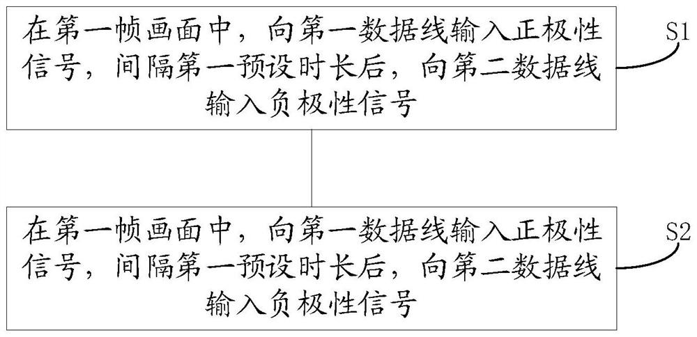
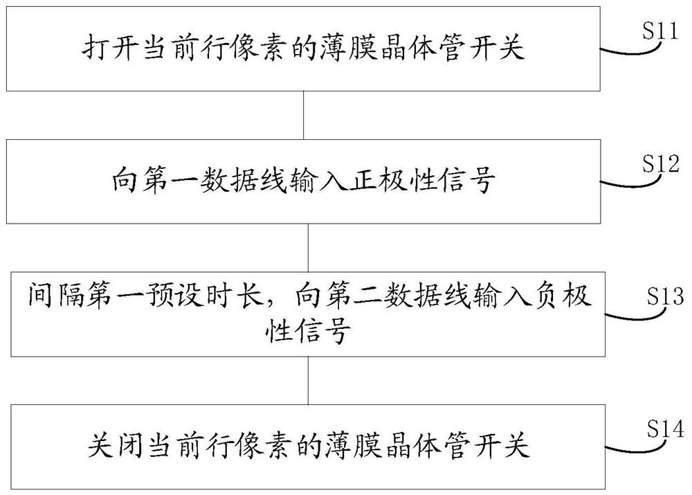
[0045] see figure 2 , figure 2 It is a schematic flowchart of a pixel chargi...


PUM


Abstract

The invention discloses a pixel charging method and a display panel. According to the pixel charging method and the display panel, in a first frame of picture, positive polarity signals are input to a part of data lines, and negative polarity signals are input to other data lines after a first preset duration, so that the phases of the positive polarity signals and the negative polarity signals are changed (the positive polarity is in the front and the negative polarity is in the back); in a second frame picture, negative polarity signals are input to a part of data lines, and positive polarity signals are input to other data lines after a second preset duration so as to change the phases of the positive polarity signals and the negative polarity signals (the negative polarity is in the front and the positive polarity is in the back); that is, in the first frame of picture, the power supply voltage derivates along with the polarity direction, and the first power supply interference occurs; in the second frame of picture, the power supply voltage deviates along with the polarity direction, and second power supply interference occurs; through mutual counteraction of two interferences, the overall charging rate is ensured to be high, and meanwhile, poor crosstalk in the horizontal direction during display can be avoided.

Description

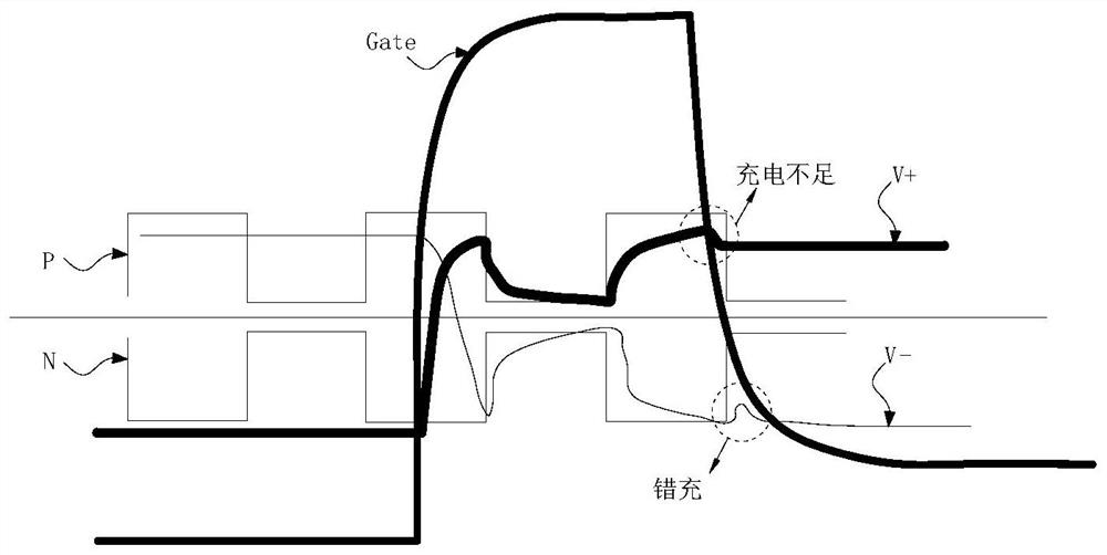
technical field [0001] The present application relates to the field of display technology, in particular to a pixel charging method and a display panel. Background technique [0002] see figure 1 , figure 1 A schematic diagram of charging pixels of an existing display panel. Such as figure 1 As shown, the current display panel has the same charging time for positive polarity and negative polarity. The positive polarity signal P and the negative polarity signal N are transmitted to the data line at the same time. Due to the long falling edge time of the gate signal Gate, there is insufficient time for the positive polarity signal P to charge the pixel V+, and the negative polarity signal N may cause errors in charging the pixel V-. Charge. Based on this, there is a time difference between the output of the positive polarity signal and the negative polarity signal, which can improve charging. [0003] However, if there is a timing difference between the output of the pos...

Claims


Application Information

Patent Timeline
Patent Type & Authority Applications(China)
IPC IPC(8): G09G3/20
CPCG09G3/20G09G2310/0254G09G3/3614G09G2320/0209G09G2310/08G09G3/3688G09G3/3648G09G2310/0251G09G2310/0248G02F1/1341G09G2300/0823G09G2340/16
Inventor 潘英一
Owner TCL CHINA STAR OPTOELECTRONICS TECH CO LTD
Learn More