Display panel and manufacturing method thereof, drive control method, and display device

A technology for display panels and driving substrates, applied in static indicators, instruments, diodes, etc., can solve the problems that affect the display performance of OLED display panels, unsaturated monochrome display, and reduce color gamut, so as to improve display quality and enhance saturation. Intensity and color gamut, the effect of reducing shine

Active Publication Date: 2022-04-08
HEFEI BOE ZHUOYIN TECH CO LTD +1
View PDF0 Cites 0 Cited by
  • Summary
  • Abstract
  • Description
  • Claims
  • Application Information

AI Technical Summary

Problems solved by technology

However, the charge generation layer has a strong electrical conductivity, which will cause the charges in the charge generation layer to be transmitted laterally, and the aging of the organic material in the pixel region will further lead to the lateral transfer of charges. Therefore, when the display panel displays a monochrome picture (ie When a solid-color picture, such as a red picture, a green picture or a blue picture), the charge transmitted laterally to the adjacent OLED will cause the adjacent OLED pixel to light up, resulting in poor crosstalk, making the monochrome display unsaturated, reducing the color gamut, etc., affecting The display performance of the OLED display panel

Method used


Image

  • Display panel and manufacturing method thereof, drive control method, and display device
  • Display panel and manufacturing method thereof, drive control method, and display device
  • Display panel and manufacturing method thereof, drive control method, and display device

Examples


no. 1 example

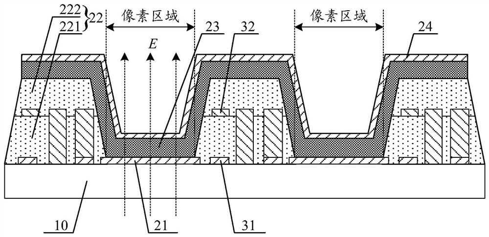
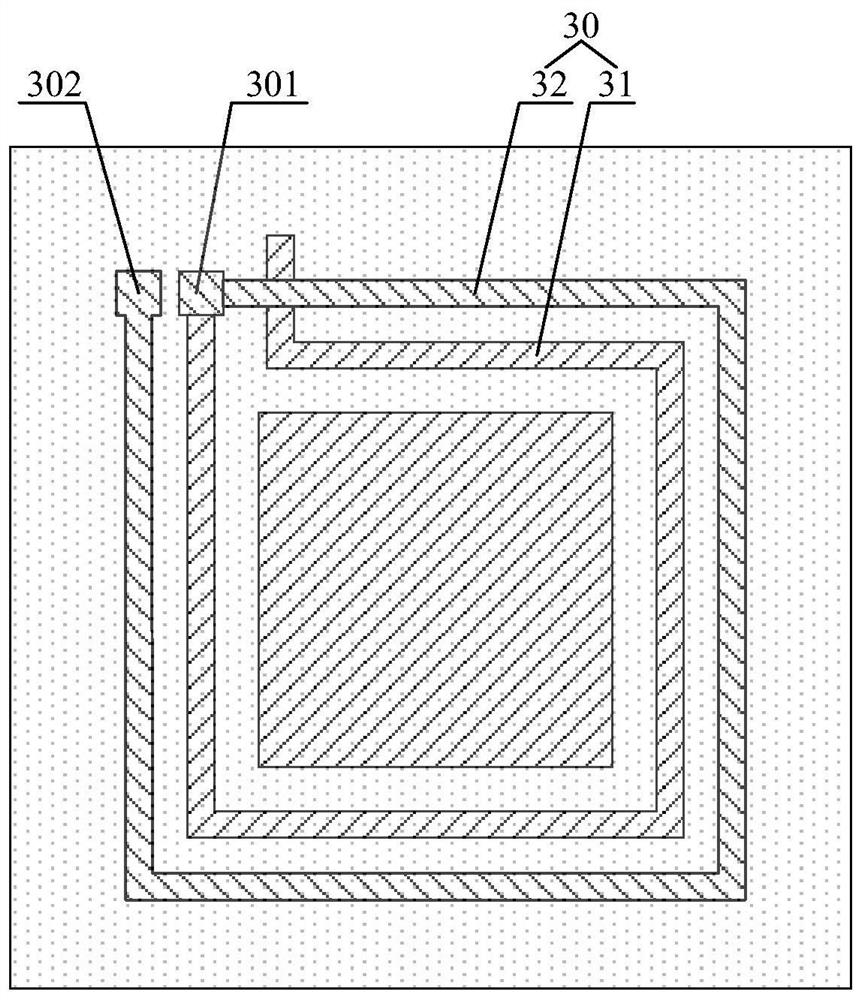
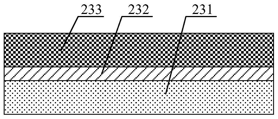
[0048] figure 1 It is a schematic cross-sectional structure diagram of the display panel according to the first embodiment of the present invention. Such as figure 1As shown, the display panel includes a plurality of pixel regions, the display panel includes a driving substrate 10, a first electrode 21 disposed on the driving substrate 10 and located in the pixel region, and a pixel defining layer 22 disposed on the first electrode 21, the pixel defining layer 22 defines a pixel area. The display panel further includes a light emitting structure layer 23 disposed on the pixel defining layer 22 and a second electrode 24 disposed on the light emitting structure layer 23 . The display panel also includes a magnetic field E arranged in at least one pixel area, the direction of the magnetic field forms a certain angle with the plane where the driving substrate 10 is located, and the magnetic field is used to suppress the lateral transfer of charges in the light-emitting structure...

no. 2 example

[0089] Based on the inventive concepts of the aforementioned embodiments, an embodiment of the present invention further provides a display device, which includes the display panel using the aforementioned embodiments. The display device can be any product or component with a display function such as a mobile phone, a tablet computer, a television, a monitor, a notebook computer, a digital photo frame, a navigator, and the like.


PUM


Abstract

The invention discloses a display panel, a preparation method thereof, a driving control method, and a display device. The display panel includes a driving substrate, a first electrode arranged on the driving substrate and located in the pixel area, and a pixel defining layer arranged on the first electrode and defining the pixel area, and the display panel also includes an electrode arranged on the pixel area. The light emitting structure layer on the pixel defining layer, the second electrode disposed on the light emitting structure layer, and the magnetic field disposed in at least one of the pixel regions, the direction of the magnetic field forms a certain angle with the plane where the driving substrate is located . In the display panel, when the charges in the light-emitting structure layer are transported laterally, the magnetic field will generate a Lorentz force on the charges, changing the direction of movement of the charges, causing the charges to perform a spiral motion, greatly increasing the travel of the charges, and limiting the lateral transfer of the charges. , reducing the brightness of adjacent pixels, avoiding bad crosstalk, and improving the display quality of the display panel.

Description

technical field [0001] The invention relates to the field of display technology, in particular to a display panel, a manufacturing method thereof, a driving control method, and a display device. Background technique [0002] The organic light emitting diode display panel (Organic Light Emitting Diode, OLED) has the characteristics of all solid state, self-illumination, high contrast ratio, wide viewing angle, etc., and is a next-generation flat panel display panel after the liquid crystal display panel. [0003] Large-size OLED display panels generally use a combination of white OLED and color film to generate red, green and blue light. White light OLEDs usually use stacked 2-layer or 3-layer sub-light-emitting layers to generate white light, and charge generation layers (CGL) are used to connect adjacent sub-light-emitting layers to reduce the voltage of white light OLED devices. The charge generation layer needs to be made of a material with strong conductivity. At presen...

Claims


Application Information

Patent Timeline
Patent Type & Authority Patents(China)
IPC IPC(8): H01L27/32G09G3/3225
CPCG09G3/3225H10K59/32H10K59/122H01F7/20H01F5/003H10K59/35H10K59/38H10K50/85H05B45/60G09G2320/0209G09G2320/0242H10K71/00
Inventor 万想
Owner HEFEI BOE ZHUOYIN TECH CO LTD
Why Eureka
Try Eureka