TFT-LCD (thin film transistor-liquid crystal display) panel and driving method thereof

A panel and gate drive technology, applied in nonlinear optics, instruments, optics, etc., can solve the problems of large GOA signal delay, increased panel logic power consumption, product design failure, etc., and achieve the effect of reducing logic power consumption

Inactive Publication Date: 2012-09-19
BOE TECH GRP CO LTD
View PDF4 Cites 21 Cited by
  • Summary
  • Abstract
  • Description
  • Claims
  • Application Information

AI Technical Summary

Problems solved by technology

[0008] From the formula, we can see that the power consumption of the GOA part is proportional to the frequency f of the clock pulse signal when the high level and low level of the clock pulse signal are determined. For example, the panel refresh frequency is driven by 60Hz When changing to 120Hz drive, the power consumption of the GOA part will double. For panels with specific requirements for logic power consumption, such changes sometimes even lead to product design failures
[0009] Since GOA technology adopts TFT technology, compared with the complementary metal oxide semiconductor (Complementary Metal Oxide Semiconductor (CMOS) technology used in the traditional Chip On Film (COF) method, in addition to the logic power consumption of the panel, there will be In addition to a certain increase, the delay of the GOA signal is greater than that of the COF method, so when the refresh rate of the panel is increased, the charging rate of the pixel cannot be met.

Method used


Image

  • TFT-LCD (thin film transistor-liquid crystal display) panel and driving method thereof
  • TFT-LCD (thin film transistor-liquid crystal display) panel and driving method thereof
  • TFT-LCD (thin film transistor-liquid crystal display) panel and driving method thereof

Examples


Embodiment Construction

[0028] The TFT-LCD panel and its driving method according to the embodiments of the present invention will be described in detail below with reference to the accompanying drawings.

[0029] It should be clear that the described embodiments are only some of the embodiments of the present invention, not all of them. Based on the embodiments of the present invention, all other embodiments obtained by persons of ordinary skill in the art without creative efforts fall within the protection scope of the present invention.

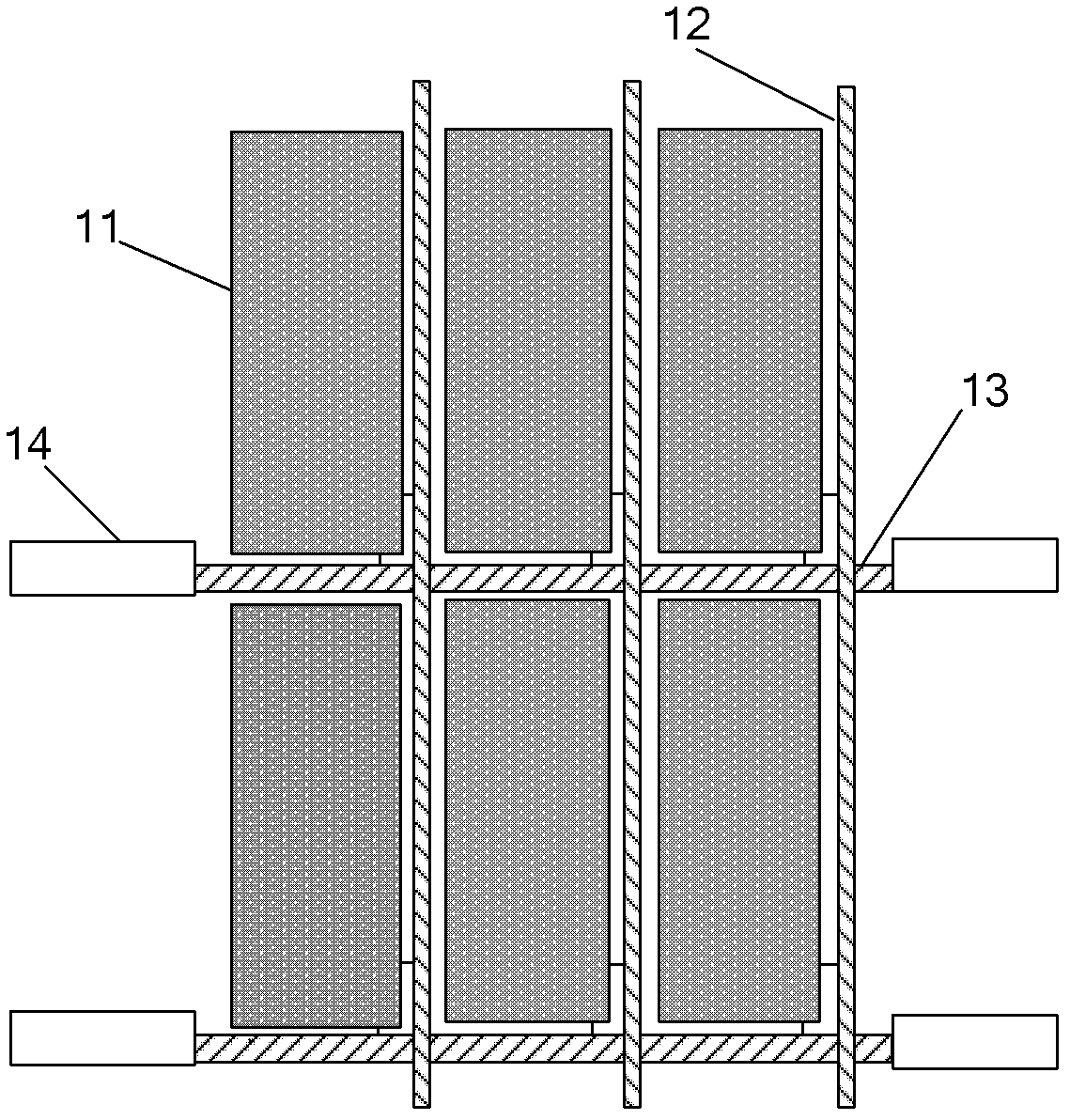
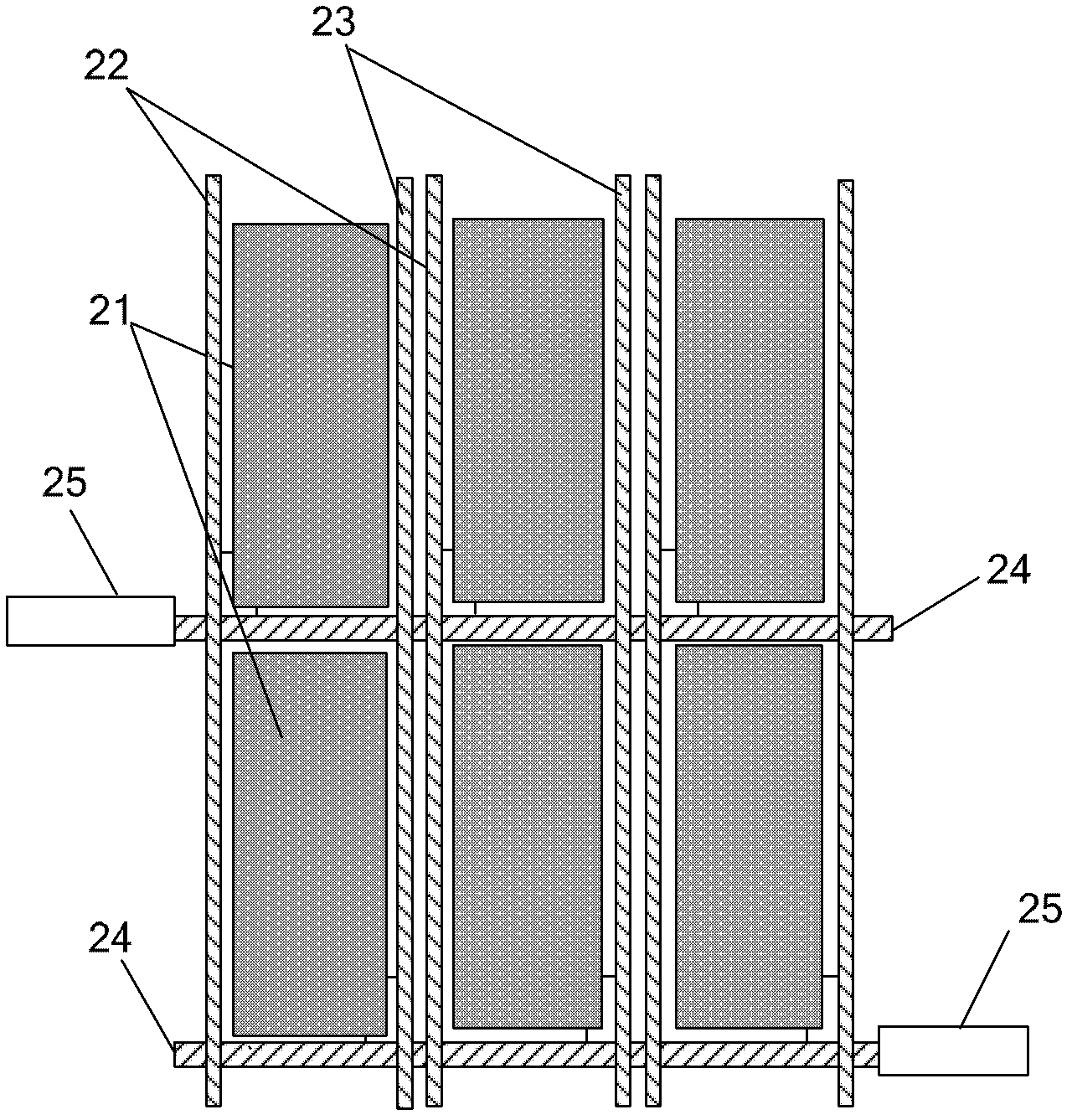
[0030] Such as figure 2 As shown, the embodiment of the present invention provides a TFT-LCD panel, including: several sub-pixel units 21 defined by the crossing of rows of gate lines 24 and columns of data lines, each row of gate lines 24 is connected to one for providing gate drive signals GOA Unit 25;

[0031] Both sides of each column of sub-pixel units are respectively provided with a first data line 22 and a second data line 23 that provide data signals ...


PUM


Abstract

The invention discloses a TFT-LCD (thin film transistor-liquid crystal display) panel and a driving method thereof and relates to the field of liquid crystal displays. Panel power consumption cannot be increased while requirements of pixel charge rate can be met at high refresh frequency. The TFT-LCD panel comprises a plurality of sub-pixel units crosswise defined by several rows of grid lines and several columns of data lines, each row of grid lines is connected with a GOA (gate driver on array) unit used for providing grid driving signals, a first data line and a second data line which are used for providing data to the sub-pixel units in each column are arranged on two sides of each column of the sub-pixel units respectively, each two adjacent sub-pixel units in each column are respectively connected with the first data line and the second data line, each two GOA units provide the same grid driving signals, and one of the two GOA units providing the same grid driving signals is connected with the grid lines in odd rows while the other of the two GOA units is connected with the grid lines in even rows.

Description

technical field [0001] The invention relates to the field of liquid crystal displays, in particular to a Thin Film Transistor Liquid Crystal Display (TFT-LCD for short) panel and a driving method thereof. Background technique [0002] With the development of the TFT-LCD industry, the competition of TFT-LCD products is becoming increasingly fierce, and all manufacturers are adopting new technologies to reduce the cost of products, thereby improving the competitiveness of their products in the market. Gate Driver on Array (GOA for short) technology is a typical representative of these new technologies. [0003] GOA technology is to integrate the gate driver unit on the array substrate to form the GOA unit, so that the gate driver IC (Gate Driver IC) part can be saved, and the product cost can be reduced in terms of material cost and process steps. [0004] In the process of realizing the present invention, the inventor finds that there are at least the following problems in t...

Claims


Application Information

Patent Timeline
Patent Type & Authority Applications(China)
IPC IPC(8): G02F1/1362G02F1/1368G02F1/133G09G3/36
CPCG02F1/13306G09G3/3677G09G3/3688G02F1/1362G09G2330/021G09G3/36G09G2310/0205G02F1/136G02F1/1368G02F1/133G02F1/136286
Inventor 吕敬彭宽军张玉婷
Owner BOE TECH GRP CO LTD
Why Eureka
Try Eureka