Wafer defect detection system and detection method thereof

A defect detection and wafer technology, applied in optical testing flaws/defects, measuring devices, material analysis by optical means, etc., can solve the problems of discontinuous wafer inspection process, wafer damage, and low inspection efficiency.

Inactive Publication Date: 2022-03-04
王建楠
View PDF0 Cites 4 Cited by
  • Summary
  • Abstract
  • Description
  • Claims
  • Application Information

AI Technical Summary

Problems solved by technology

[0003] In this way, during the inspection process, manual participation is required throughout the entire process, and the wafer needs to be manually placed in the inspection area. After the inspection is completed, the operator will then take out the wafer. In this process, manual participation must be avoided. The wafer is damaged, and there is a time diff

Method used


Image

  • Wafer defect detection system and detection method thereof
  • Wafer defect detection system and detection method thereof
  • Wafer defect detection system and detection method thereof

Examples


Embodiment Construction

[0030] The following will clearly and completely describe the technical solutions in the embodiments of the present invention with reference to the accompanying drawings in the embodiments of the present invention. Obviously, the described embodiments are only some, not all, embodiments of the present invention. Based on the embodiments of the present invention, all other embodiments obtained by persons of ordinary skill in the art without making creative efforts belong to the protection scope of the present invention.

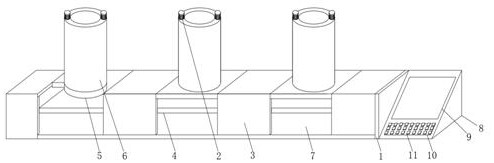
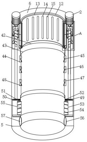
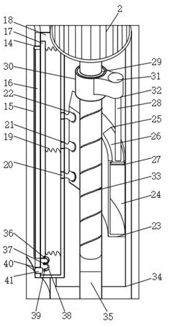
[0031] Such as Figure 1-4 As shown, the present invention provides a technical solution: a wafer defect detection system, including a hollow operation box 1, a detection terminal 8 is fixedly connected to the right side of the hollow operation box 1, and a display screen 9 is arranged on the top of the detection terminal 8. An operation panel 10 is fixedly connected below the top of the detection terminal 8, and an operation button 11 is arranged on the opera...


PUM


Abstract

The invention relates to the technical field of wafer defect detection, and discloses a detection method of a wafer defect detection system, the wafer defect detection system comprises a hollow operation box, and the right side of the hollow operation box is fixedly connected with a detection terminal. When the wafers are detected, the stacked wafers are placed in the vertical conveying mechanism, when the lower pressing plate and the sealing sleeve move to the position above the inner cavity of the pressure cavity, gas in the inner cavity of the pressure cavity is pumped out from the three installation gas rings, and therefore the wafer conveying device has the advantages that in the process of conveying the wafers downwards, the gas in the inner cavity of the pressure cavity is pumped out from the three installation gas rings; a plurality of wafers can be placed in a centralized mode, the wafers can be fixed in the radial direction by means of the air pressure effect and utilizing the protruding strips to move outwards, the wafers placed at the lowest position are limited by the limiting head due to the fact that the distance exists between the protruding strips and the limiting head, and then the wafers can be blocked in a centralized mode. And the effect of centralized discharging can be achieved.

Description

technical field [0001] The invention relates to the technical field of wafer detection, in particular to a wafer defect detection system and a detection method thereof. Background technique [0002] At present, there are two commonly used wafer particle detection methods: manual detection method, relying on a microscope to manually detect wafer particles under sterile and dust-free conditions, and detect defects and particles on the wafer surface in time to prevent cleanliness Insufficient wafers enter the machine to ensure the process quality of wafer manufacturing, but manual inspection has the disadvantages of low efficiency and large errors; optical inspection methods use optical scattering intensity measurement technology to detect the presence or absence of particles on the wafer surface, The spatial distribution of particles on the wafer surface has the advantages of not destroying the cleanliness of the wafer surface and real-time detection. It is more and more favor...

Claims


Application Information

Patent Timeline
IPC IPC(8): G01N21/95
CPCG01N21/9505
Inventor 王建楠
Owner 王建楠
Why Eureka
Try Eureka