Lighting apparatus using LED wafer array and method thereof

A technology of lighting equipment and chips, which is applied in the direction of lighting and heating equipment, lighting devices, components of lighting devices, etc., to achieve the effect of reducing manufacturing costs

Pending Publication Date: 2022-03-18
国际设计中心韩国有限公司
View PDF0 Cites 0 Cited by
  • Summary
  • Abstract
  • Description
  • Claims
  • Application Information

AI Technical Summary

Problems solved by technology

No one has yet developed inorganic GaN-based lighting devices and brought this delivery technology to market

Method used


Image

  • Lighting apparatus using LED wafer array and method thereof
  • Lighting apparatus using LED wafer array and method thereof
  • Lighting apparatus using LED wafer array and method thereof

Examples


Embodiment Construction

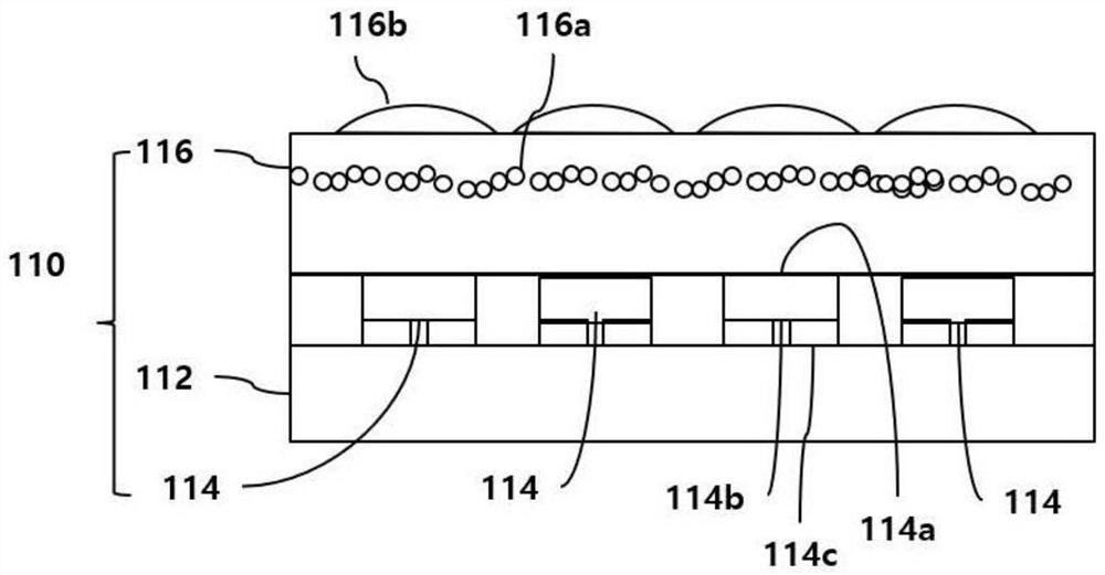
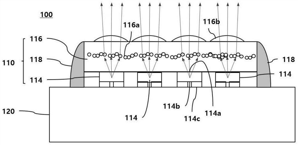
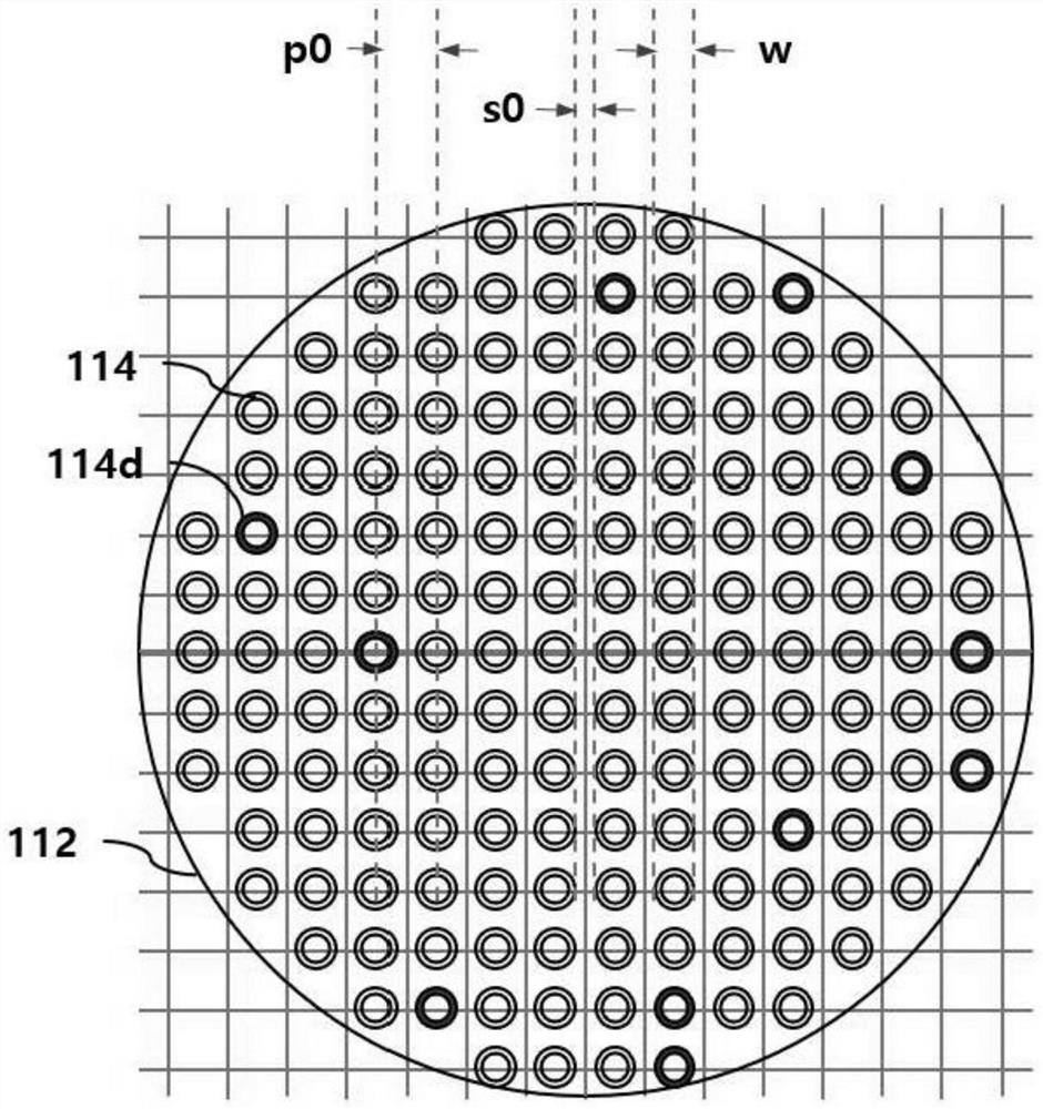
[0031] Regarding the exemplary embodiments of the present invention disclosed in the specification, specific structural or functional descriptions are shown only for the purpose of illustrating the exemplary embodiments of the present invention, and the exemplary embodiments of the present invention can be implemented in various shapes, It should not be construed as limiting the exemplary embodiments of the invention disclosed in the specification.

[0032] The present invention may be embodied in various alternative forms and may have various shapes, therefore, specific exemplary embodiments are shown in the drawings and described in the description. However, the description should not be construed as being limited to the exemplary embodiments set forth herein, and the description should be construed to include all changes, modifications or substitutions falling within the spirit and scope of the invention. In describing each figure, the same reference numerals are used for t...


PUM

PropertyMeasurementUnit
sizeaaaaaaaaaa
sizeaaaaaaaaaa
thicknessaaaaaaaaaa

Abstract

Disclosed is a lighting device using a light emitting element wafer array, the lighting device comprising: a substrate; a plurality of light emitting element wafer arrays attached to the substrate and arranged in a matrix shape, the light emitting element wafer including a light emitting surface and an electrode forming surface facing the light emitting surface, the flip chip bonding electrode being formed on the electrode forming surface; and a transparent support layer covering light-emitting surfaces of the plurality of light-emitting element wafers and fixing the plurality of light-emitting element wafers at a constant light source interval, the transparent support layer including a fluorescent material that absorbs light emitted through the light-emitting surfaces to change a wavelength of the light.

Description

technical field [0001] The present invention relates to a lighting device using a light-emitting element chip array and a method thereof, and more particularly, to a lighting device using a light-emitting element chip array and a method thereof, wherein, by directly using a wafer-level light-emitting element (LED) Wafers are not required to be sorted into good / bad to manufacture the light source module, thereby reducing the manufacturing cost. Background technique [0002] For example, light-emitting elements such as light-emitting diodes (LEDs) are one of semiconductor elements that convert electrical energy into light, and are attracting attention as next-generation light sources that replace conventional fluorescent lamps and incandescent lamps. [0003] Since light-emitting diodes generate light using a potential difference of semiconductor elements, light-emitting diodes have environmentally friendly characteristics such as longer lifespan, fast response speed, and low ...

Claims


Application Information

Patent Timeline
Patent Type & Authority Applications(China)
IPC IPC(8): H01L25/075H01L33/50H01L33/54H01L33/58F21K9/69F21K9/90F21Y115/10
CPCH01L25/0753H01L33/50H01L33/54H01L33/58F21K9/69F21K9/90F21Y2115/10F21V5/00F21K9/60H01L33/62H01L33/502H01L33/38H01L2933/0066H01L2933/0016H01L2933/0041H01L33/005F21V5/004
Inventor 金昶煜
Owner 国际设计中心韩国有限公司
Why Eureka
Try Eureka