Check patentability & draft patents in minutes with Patsnap Eureka AI!

MCU double-wire debugging circuit and MCU double-wire debugging method

A technology for debugging circuits and debuggers, which is applied in the fields of electrical digital data processing, instruments, calculations, etc., can solve problems such as difficulty in guaranteeing reliability and debugging speed, difficult technical implementation, and no unified implementation plan, etc., to achieve rich debugging functions, Improving communication efficiency, richness and outstanding effect

Pending Publication Date: 2022-03-29
佛山巨晟微电子有限公司
View PDF0 Cites 0 Cited by
  • Summary
  • Abstract
  • Description
  • Claims
  • Application Information

AI Technical Summary

Problems solved by technology

Among them, the four-wire debugging interface is generally a standard JTAG interface, which needs to occupy four IO interfaces in the chip, so these four IO interfaces cannot be used as functional PINs during the debugging process, which is not friendly to the simulation debugging during the solution development process. , and four wires will increase the hardware complexity during debugging
Although the single-line debugging interface minimizes the IO occupancy rate, it is difficult to implement technically, and its reliability and debugging speed are difficult to guarantee.
Two-wire debugging is the most mainstream debugging mode in the market at present, but there is no unified implementation plan. The SWD debugging interface of ARM core is the most popular, but it is only applicable to chips using ARM core.

Method used


Image

  • MCU double-wire debugging circuit and MCU double-wire debugging method
  • MCU double-wire debugging circuit and MCU double-wire debugging method
  • MCU double-wire debugging circuit and MCU double-wire debugging method

Examples


Embodiment Construction

[0021] This part will describe the specific embodiment of the present invention in detail, and the preferred embodiment of the present invention is shown in the accompanying drawings. Each technical feature and overall technical solution of the invention, but it should not be understood as a limitation on the protection scope of the present invention.

[0022] In the description of the present invention, several means one or more, and multiple means two or more. Greater than, less than, exceeding, etc. are understood as not including the original number, and above, below, within, etc. are understood as including the original number. If the description of the first and second is only for the purpose of distinguishing the technical features, it cannot be understood as indicating or implying the relative importance or implicitly indicating the number of the indicated technical features or implicitly indicating the order of the indicated technical features relation.

[0023] In t...


PUM


Abstract

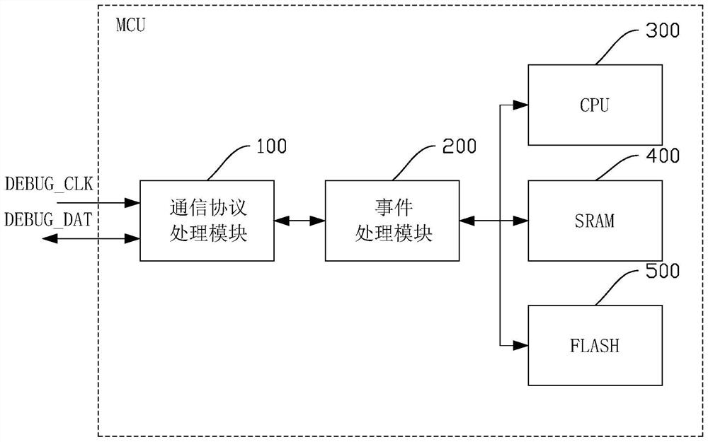
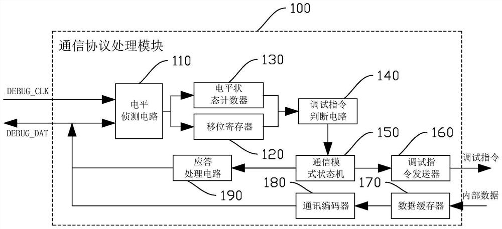
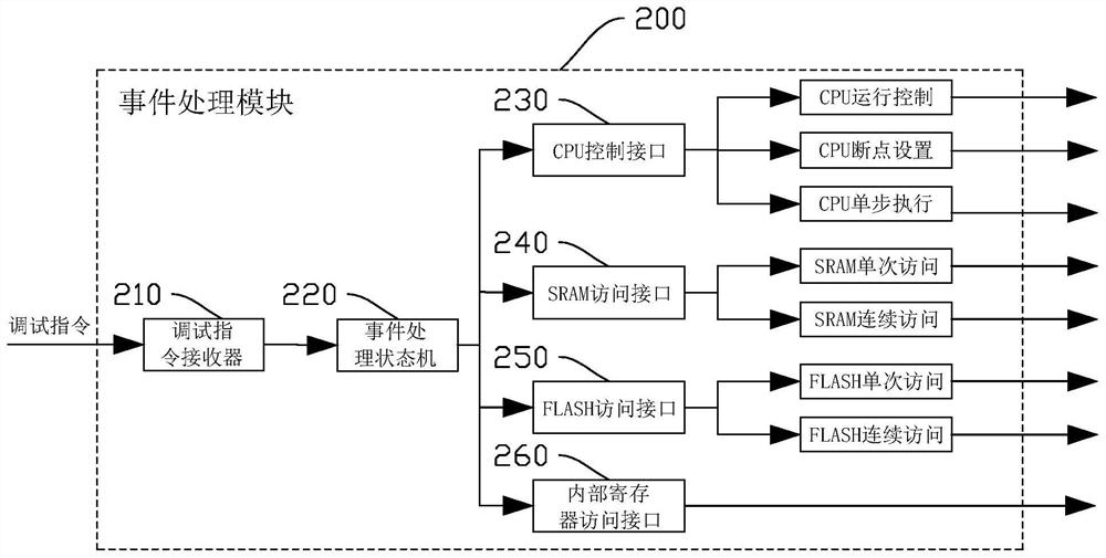
The invention discloses an MCU double-wire debugging circuit and an MCU double-wire debugging method. The MCU double-wire debugging circuit comprises a communication protocol processing module and an event processing module. Wherein the communication protocol processing module is used for performing information interaction with an off-chip debugger according to a communication protocol; the event processing module is electrically connected with the communication protocol processing module, and the event processing module is used for executing corresponding actions according to the received debugging instruction, including at least one of controlling a CPU (Central Processing Unit) of the MCU, accessing an SRAM (Static Random Access Memory) in the MCU and accessing a FLASH in the MCU, and transmitting internal data to the debugger through the communication protocol processing module. According to the MCU double-wire debugging circuit, the communication protocol processing module provides a high-reliability communication interaction mode, and communication can be completed only by using two IO interfaces; and the event processing module provides abundant debugging functions, so that software developers can debug programs conveniently.

Description

technical field [0001] The invention relates to the technical field of chip debugging, in particular to an MCU two-wire debugging circuit and an MCU two-wire debugging method. Background technique [0002] With the rapid development of chip design technology, MCU chips have higher and higher requirements for pin functions, and solution providers tend to use chips with fewer PINs to achieve richer application functions. [0003] There are three mainstream debugging interfaces for MCU chips in the market: four-wire debugging, two-wire debugging and single-wire debugging. Among them, the four-wire debugging interface is generally a standard JTAG interface, which needs to occupy four IO interfaces in the chip. As a result, these four IO interfaces cannot be used as functional PINs during the debugging process, which is not friendly to the simulation debugging during the solution development process. , and four lines will increase the hardware complexity in the debugging process...

Claims


Application Information

Patent Timeline
IPC IPC(8): G06F11/263G06F11/273
CPCG06F11/263G06F11/2733
Inventor 王浩远
Owner 佛山巨晟微电子有限公司
Features
  • R&D
  • Intellectual Property
  • Life Sciences
  • Materials
  • Tech Scout
  • Unparalleled Data Quality
  • Higher Quality Content
  • 60% Fewer Hallucinations
Learn More