Backboard

A backplane and substrate substrate technology, applied in the direction of electrical components, electrical solid devices, circuits, etc., can solve the problem of not being able to save the pixel area, and achieve the effect of saving the pixel area

Pending Publication Date: 2022-03-29
BOE TECH GRP CO LTD
View PDF0 Cites 0 Cited by
  • Summary
  • Abstract
  • Description
  • Claims
  • Application Information

AI Technical Summary

Problems solved by technology

[0002] In the prior art, when making a display technology field or a 3D printing technology backplane, when the size of the pixel area occupied by the pixel structure in the backplane is small, the pixel area cannot be saved, and the rational layout cannot be made through the saved pixel area. Driver Transistors in Pixel Structures

Method used


Image

  • Backboard
  • Backboard
  • Backboard

Examples


Embodiment Construction

[0025] The following will clearly and completely describe the technical solutions in the embodiments of the present invention with reference to the accompanying drawings in the embodiments of the present invention. Obviously, the described embodiments are only some, not all, embodiments of the present invention. Based on the embodiments of the present invention, all other embodiments obtained by persons of ordinary skill in the art without making creative efforts belong to the protection scope of the present invention.

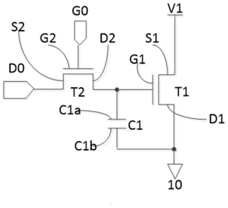
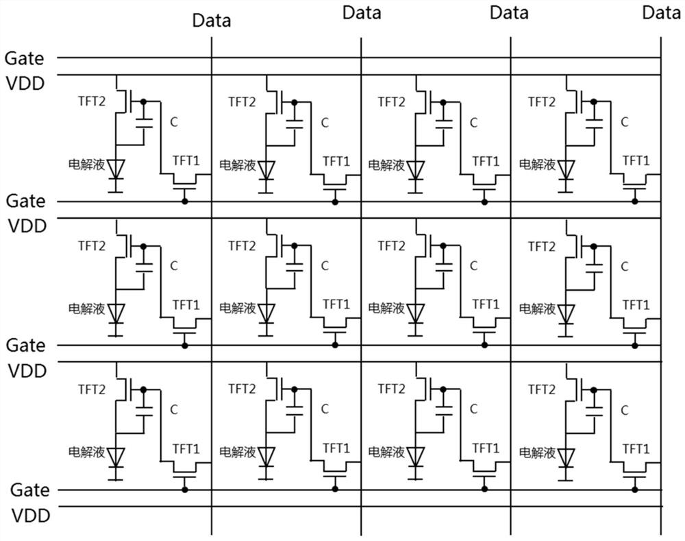
[0026] The backplane provided by the present application can at least be used as a printing backplane in a 3D printing system. The backplane contains printing anodes distributed in an array, and the backplane drives the anodes to realize 3D printing. Or the backplane provided by the present application can at least be used in the field of display to drive pixel electrodes to realize liquid crystal display or OLED display.

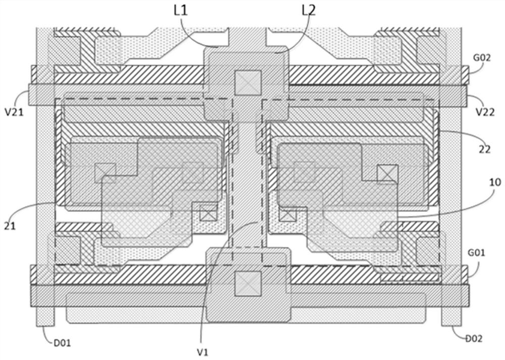
[0027] The backplane described in th...


PUM


Abstract

The invention provides a back plate. The back plate comprises a substrate, grid lines, data lines, power lines and pixel structures, wherein the grid lines, the data lines and the power lines are staggered in rows and columns, and the pixel structures are distributed in an array mode. The pixel structure comprises a driving transistor, a switching transistor connected with the driving transistor and a pixel electrode connected with the driving transistor, the grid line and the data line are respectively connected with the switching transistor, and the power line is connected with the driving transistor; in the same row of pixel structures or the same column of pixel structures, a power line is arranged between the (2n-1) th pixel structure and the (2n) th pixel structure, the power line is connected with a source electrode of the driving transistor in the (2n-1) th pixel structure, and the power line is connected with a source electrode of the driving transistor in the (2n) th pixel structure; n is a positive integer greater than or equal to 1. According to the invention, the pixel area can be saved, so that the driving transistors in the pixel structure can be reasonably arranged through the saved pixel area.

Description

technical field [0001] The present invention relates to the field of display technology or the field of 3D printing technology, in particular to a backplane. Background technique [0002] In the prior art, when making a display technology field or a 3D printing technology backplane, when the size of the pixel area occupied by the pixel structure in the backplane is small, the pixel area cannot be saved, and the rational layout cannot be made through the saved pixel area. A drive transistor in a pixel structure. Contents of the invention [0003] One of the objectives of the present invention is to provide a backplane, provide a pixel structure design of the backplane, improve the driving ability of the pixel to the pixel electrode or 3D printing anode, and reduce the occupied area of ​​the pixel structure to improve the pixel resolution. [0004] The present invention provides a backplane, comprising a base substrate, grid lines arranged in staggered rows and columns, dat...

Claims


Application Information

Patent Timeline
Patent Type & Authority Applications(China)
IPC IPC(8): H01L27/12H01L27/02
CPCH01L27/1222H01L27/124H01L27/1255H01L27/0207
Inventor 郭怡彤周健孙拓许晓春
Owner BOE TECH GRP CO LTD
Why Eureka
Try Eureka