A kind of preparation method of tft array substrate, display device and tft array substrate

An array substrate and metal layer technology, applied in semiconductor devices, electrical components, circuits, etc., can solve problems such as increased process complexity, reduced storage capacitance of TFT devices, and difficulty in ensuring reliability of TFT devices, so as to increase flexibility and reduce The effect of small pixel area and guaranteed reliability

Active Publication Date: 2021-04-27
FUJIAN HUAJIACAI CO LTD
View PDF14 Cites 0 Cited by
  • Summary
  • Abstract
  • Description
  • Claims
  • Application Information

AI Technical Summary

Problems solved by technology

However, the continuous reduction of the pixel area will inevitably lead to an increase in the complexity of the process, a continuous reduction in the storage capacity of the TFT device, and even make it difficult to guarantee the reliability of the TFT device.

Method used


Image

  • A kind of preparation method of tft array substrate, display device and tft array substrate
  • A kind of preparation method of tft array substrate, display device and tft array substrate
  • A kind of preparation method of tft array substrate, display device and tft array substrate

Examples


preparation example Construction

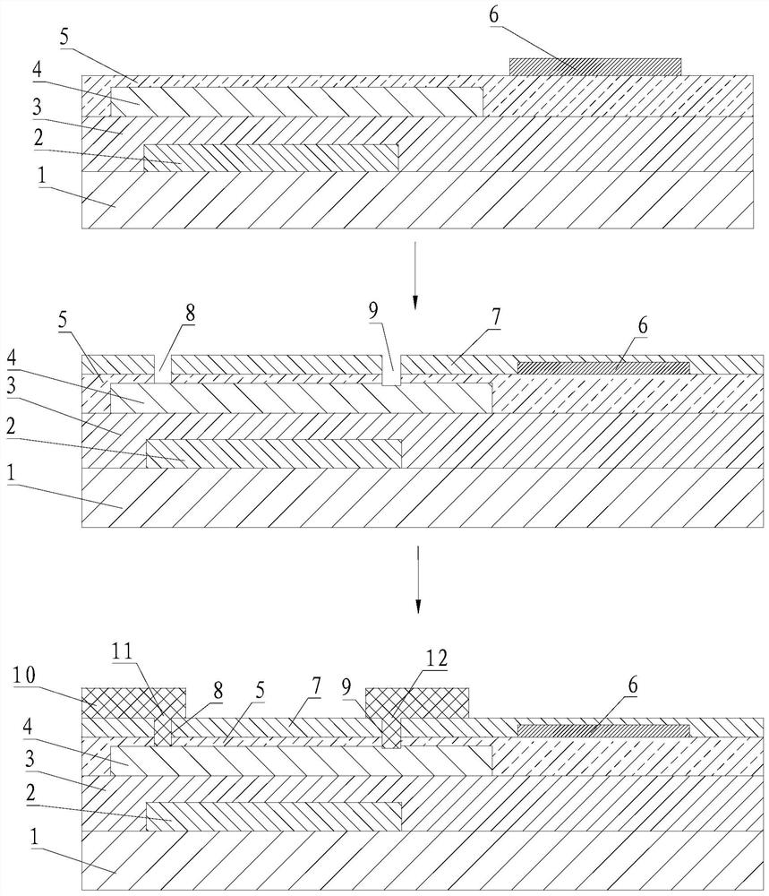
[0040] The present invention also provides a method for preparing a TFT array substrate, comprising the following steps:

[0041] Step 1: sequentially forming a gate, a gate insulating layer, an active layer and an etching barrier layer on the substrate, the gate being formed by a first metal layer;

[0042] Step 2: forming an auxiliary metal layer on the etching barrier layer;

[0043] Step 3: forming a passivation layer on the etching barrier layer and the auxiliary metal layer;

[0044]Step 4: Simultaneously pattern the passivation layer and the etching barrier layer through a patterning process to form a first via hole and a second via hole connected to the active layer;

[0045] Step 5: forming a third metal layer on the passivation layer, the third metal layer is connected to the active layer through the first via hole and the second via hole; A source electrode and a drain electrode are respectively formed at the first via hole and the second via hole.

[0046] Furth...

Embodiment 1

[0053] Please refer to figure 1 , Embodiment 1 of the present invention is:

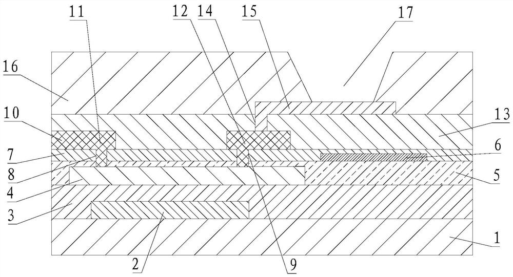
[0054] A TFT array substrate, comprising a substrate 1, a gate formed by a first metal layer 2 disposed on the substrate 1, a gate insulating layer 3 disposed on the substrate 1 and the gate, and a gate insulating layer 3 disposed on the substrate 1. The active layer 4 on the gate insulating layer 3, the etching stopper layer 5 provided on the active layer 4 and the gate insulating layer 3, the auxiliary metal layer 6 provided on the etching stopper layer 5, The passivation layer 7 disposed on the etch barrier layer 5 and the auxiliary metal layer 6 passes through the passivation layer 7 and the etch barrier layer 5 and corresponds to the upper sides of the active layer 4 respectively. The first via hole 8 and the second via hole 9, the third metal layer 10 provided on the passivation layer 7, the third metal layer 10 passes through the first via hole 8 and the second via hole 9 respectively connec...

Embodiment 2

[0059] Please refer to Figure 2 to Figure 4 , the second embodiment of the present invention is:

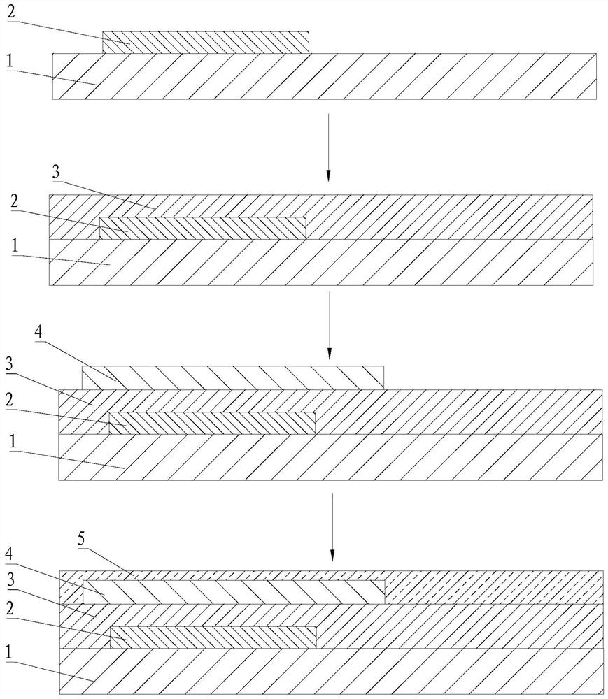
[0060] A method for preparing a TFT array substrate, comprising the steps of:

[0061] Step 1: Evaporate the first metal layer (M1) 2 on the substrate 1 by physical vapor deposition (PVD), generally with a Mo / AL / Mo sandwich layer structure, and expose (photo) after photoresist coating, according to the mask Plate (MASK) design to form the required pattern, and then etch the first metal layer (M1) 2 to form the pattern of the gate (GE);

[0062] Step 2: Evaporating a gate insulating layer (GI) 3 on the substrate treated in step 1 by chemical vapor deposition (CVD);

[0063] Step 3: Evaporate an IGZO film on the substrate treated in step 2 by PVD method, and go through exposure (photo), etching (etch) and stripping (stripe) processes; finally form the required active layer (SE)4 picture of;

[0064] Step 4: Evaporating an etching stopper layer (ES) 5 on the substrate treated i...


PUM


Abstract

The invention provides a TFT array substrate, a display device and a method for preparing a TFT array substrate. The TFT array substrate has a double-layer storage capacitor structure, which can ensure a constant capacity of the storage capacitor of the TFT device and ensure the reliability of the TFT device. , reduce the pixel area, increase the PPI of the display panel, and increase the flexibility of the layout design; in addition, by setting the auxiliary metal layer between the first metal layer and the third metal layer, the upper and lower layers of the auxiliary metal layer can be made The insulating layer is patterned through a patterning process at the same time, which can save a mask, reduce the exposure, etching and stripping processes of a patterning process, and save the process cost of the TFT array substrate; the display device provided by the present invention adopts With the above-mentioned TFT array substrate, under the same display size, the pixel distribution density of the display device is greatly improved, and the display picture is clearer.

Description

technical field [0001] The invention relates to the field of display technology, in particular to a TFT array substrate, a display device and a preparation method of the TFT array substrate. Background technique [0002] Since the display screen always has high-definition requirements, this requires the pixel area to be continuously reduced to increase the pixel distribution density (PPI). In recent years, the improvement of the pixel density (PPI) of the display panel is generally limited by the size and wiring pitch of the thin film transistor (TFT) in the pixel structure, and the PPI can be improved by reducing the size of the TFT and the wiring pitch. For example, the method of sharing electrodes is used to reduce the wiring pitch to achieve the effect of improving PPI. However, the continuous reduction of the pixel area will inevitably lead to the increase of the complexity of the process, the continuous reduction of the storage capacity of the TFT device, and even mak...

Claims


Application Information

Patent Timeline
Patent Type & Authority Patents(China)
IPC IPC(8): H01L27/32
CPCH01L27/1255H01L27/1259H01L27/1288H10K59/123H10K59/1213H10K59/1216H10K59/131
Inventor 不公告发明人
Owner FUJIAN HUAJIACAI CO LTD
Why Eureka
Try Eureka