Formation method of fin structure and formation method of FinFET device

A device and fin technology, applied in the formation of fin structures and the formation of FinFET devices, can solve problems such as bending and tilting of fin structures, and achieve the effect of improving bending or tilting and stress balance

Pending Publication Date: 2022-04-12
SHANGHAI INTEGRATED CIRCUIT EQUIP & MATERIALS IND INNOVATION CENT CO +1
View PDF0 Cites 0 Cited by
  • Summary
  • Abstract
  • Description
  • Claims
  • Application Information

AI Technical Summary

Problems solved by technology

[0004] The object of the present invention is to provide a method for forming a fin structure and a me

Method used


Image

  • Formation method of fin structure and formation method of FinFET device
  • Formation method of fin structure and formation method of FinFET device
  • Formation method of fin structure and formation method of FinFET device

Examples


Example Embodiment

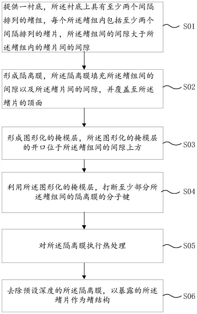
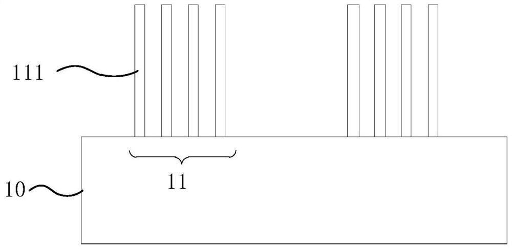
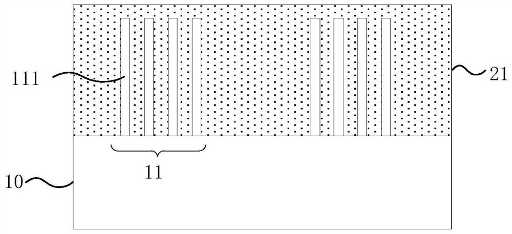
[0022] In order to make the objects, advantages and features of the present invention clearer, the present invention will be further described in detail below with reference to the accompanying drawings and specific embodiments. It should be noted that the accompanying drawings are all in a very simplified form and are not drawn to scale, and are only used to facilitate and clearly assist the purpose of explaining the embodiments of the present invention. Furthermore, the structures shown in the drawings are often part of the actual structure. In particular, each drawing needs to show different emphases, and sometimes different scales are used.

[0023] As used herein, the singular forms "a," "an," and "the" include plural referents, the term "or" is generally employed in its sense including "and / or", and the term "a number" It is usually used in the sense including "at least one", the term "at least two" is usually used in the sense including "two or more", in addition, the ...


PUM


Abstract

The invention provides a fin structure forming method and a FinFET device forming method, and the fin structure forming method comprises the steps: providing a substrate which is provided with at least two fin groups which are arranged at intervals; forming an isolation film, and filling the fins and the fin group; forming a patterned mask layer, wherein an opening of the patterned mask layer exposes the isolating film between the fin groups; breaking molecular bonds of at least part of the isolating membrane by using the patterned mask layer; performing heat treatment on the isolating membrane; and removing the isolating film at a preset depth to enable the exposed fins to be fin structures. According to the heat treatment method, the molecular bonds of at least part of the isolating membranes among the fin groups are broken, so that the expansion rate of the isolating membranes among the fin groups during heat treatment is adjusted, the stress of the isolating membranes on the two sides of the fins in the fin groups after heat treatment is relatively balanced, and the problem that the fins are bent or inclined is solved.

Description

technical field [0001] The invention relates to the technical field of integrated circuit manufacturing, in particular to a method for forming a fin structure and a method for forming a FinFET device. Background technique [0002] With the continuous development of semiconductor technology, traditional planar devices have been difficult to meet people's demand for high-performance devices. Fin-Field-Effect-Transistor (FinFET) is a three-dimensional device, including fins formed vertically on the substrate and gate structures covering both sides of the fins. This design can greatly improve The circuit controls and reduces the leakage current, and can also greatly shorten the gate length of the transistor. [0003] However, in the formation process of the fin structure (fin) of the FinFET device, the deformation (bending or tilting) of the fin is very easy to occur, which is not conducive to the subsequent process (such as the formation of the source-drain structure in the fi...

Claims


Application Information

Patent Timeline
IPC IPC(8): H01L21/336H01L29/10
Inventor 刘云珍
Owner SHANGHAI INTEGRATED CIRCUIT EQUIP & MATERIALS IND INNOVATION CENT CO
Why Eureka
Try Eureka