Chip test mode switching method and system

A test mode and mode switching technology, applied in the field of testing, can solve problems such as increased difficulty, inability to switch, and reduced chip test coverage, so as to achieve the effect of improving coverage and reliability

Pending Publication Date: 2022-04-29
上海泰矽微电子有限公司 +1
View PDF1 Cites 2 Cited by
  • Summary
  • Abstract
  • Description
  • Claims
  • Application Information

AI Technical Summary

Problems solved by technology

There are two problems in this scheme: one is that the test mode can only be entered within the monitoring time window, although the probability of false triggering is reduced, but it also increases the difficulty of entering the test mode, which requires a very accurate matching window; Cannot switch between different test modes after test mode
[0007] 2. Only supports functional test mode and SCAN Mode logic, that is, the CPU is bypassed, and the bus read and write commands are received through SPIS; while in SCAN mode, the 3 pins of SPIS cannot be reused as scan pins
[0008] 3. When used for ATE test (such as SCAN test), the SPIS module cannot be detected, resulting in reduced test coverage of the entire chip
[0009] 4. The preset characteristic value has the problem of low reliability
When SPIS is used as a normal interface, there is no guarantee that the preset characteristic value will not be received, especially when an exception occurs
This will cause the chip to enter test mode by mistake and bypass the CPU, causing system exceptions and crashes
This method will affect the normal function of the chip

Method used


Image

  • Chip test mode switching method and system
  • Chip test mode switching method and system
  • Chip test mode switching method and system

Examples


Embodiment Construction

[0080] The technical solution in this application will be described in further detail below in conjunction with the accompanying drawings.

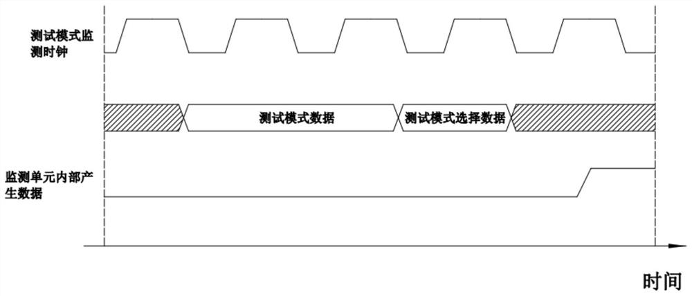
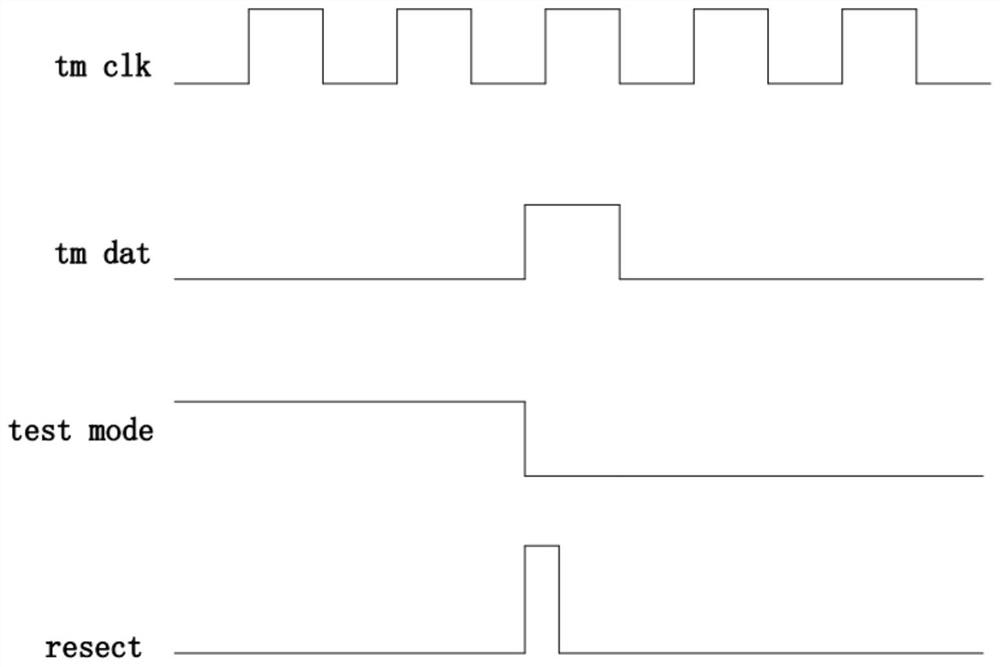
[0081] The chip test mode switching method provided by the embodiment of the present application uses the test mode data and test mode selection data to guide the chip into the test mode. The specific method is to add a monitoring unit to the chip, and the test mode issued by the tester The data is sent to the monitoring unit for judgment, and then the chip is guided into the corresponding test mode according to the test mode selection type data.

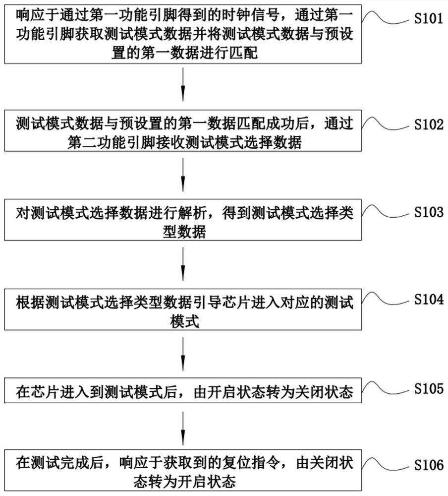
[0082] see figure 1 and figure 2 , the embodiment of the present application provides a chip test mode switching method, which is applied to the monitoring unit in the chip and multiplexes the two function pins of the chip, including the following steps:

[0083] S101, in response to the clock signal obtained through the first function pin, acquire test mode data through the first function p...


PUM


Abstract

The embodiment of the invention relates to a chip test mode switching method and system, and the method is applied to a monitoring unit in a chip, and the method comprises the steps: obtaining test mode data through a first function pin, and carrying out the matching of the test mode data with preset first data; after successful matching, receiving and analyzing test mode selection data through the second function pin to obtain test mode selection type data, and guiding the chip to enter a corresponding test mode according to the test mode selection type data; after the chip enters the test mode, the monitoring unit is converted from the on state to the off state, after the test is completed, the monitoring unit is converted from the off state to the on state, and the first function pin and the second function pin can be reused as test pins in the test mode. According to the chip test mode switching method and system provided by the embodiment of the invention, the chip can accurately enter the test mode and can stably run in the test mode on the premise of not increasing chip pins.

Description

technical field [0001] The present application relates to the technical field of testing, in particular to a chip testing mode switching method and system. Background technique [0002] The chip can use dedicated pins or functional pins to enter the test mode. The advantage of dedicated pins is that they are independent of functional pins and will not introduce possible misoperations. The disadvantage is that special pins need to be added, which will increase additional tests. cost. The advantage of the method of multiplexing pins is that it can reduce the number of pins, but the disadvantage is that it may enter the test mode by mistake in the functional test mode, which will affect the test process. [0003] In a scheme of the prior art, the chip logic generates an internal delayed reset signal under the action of power-on or external pins. Within the delay window, the monitoring logic is in the working state, and other logics are in the reset state. When the monitoring l...

Claims


Application Information

Patent Timeline
Patent Type & Authority Applications(China)
IPC IPC(8): G01R31/3185G01R31/3177
CPCG01R31/3185G01R31/318533G01R31/3177
Inventor 潘明方陈立新熊海峰
Owner 上海泰矽微电子有限公司
Why Eureka
Try Eureka